FDMA420NZ Fairchild Semiconductor, FDMA420NZ Datasheet

MOSFET N-CH 20V 5.7A MICROFET

FDMA420NZ

Manufacturer Part Number
FDMA420NZ
Description
MOSFET N-CH 20V 5.7A MICROFET
Manufacturer
Fairchild Semiconductor
Series
PowerTrench®r
Type
Power MOSFETr
Datasheet

Specifications of FDMA420NZ

Fet Type
MOSFET N-Channel, Metal Oxide
Fet Feature
Logic Level Gate
Rds On (max) @ Id, Vgs
30 mOhm @ 5.7A, 4.5V
Drain To Source Voltage (vdss)
20V
Current - Continuous Drain (id) @ 25° C
5.7A
Vgs(th) (max) @ Id
1.5V @ 250µA
Gate Charge (qg) @ Vgs
12nC @ 4.5V
Input Capacitance (ciss) @ Vds
935pF @ 10V
Power - Max
2.4W
Mounting Type
Surface Mount
Package / Case
6-MLP, 6-MicroFET™
Configuration
Single Quad Drain
Transistor Polarity
N-Channel
Resistance Drain-source Rds (on)
0.03 Ohm @ 4.5 V
Drain-source Breakdown Voltage
20 V
Gate-source Breakdown Voltage
+/- 12 V
Continuous Drain Current
5.7 A
Power Dissipation
900 mW
Maximum Operating Temperature
+ 150 C
Mounting Style
SMD/SMT
Minimum Operating Temperature
- 55 C
Number Of Elements
1
Polarity
N
Channel Mode
Enhancement
Drain-source On-res
0.03Ohm
Drain-source On-volt
20V
Gate-source Voltage (max)
±12V
Operating Temp Range
-55C to 150C
Operating Temperature Classification
Military
Mounting
Surface Mount
Pin Count
6
Package Type
MicroFET
Lead Free Status / RoHS Status
Lead free / RoHS Compliant
Other names
FDMA420NZTR

Available stocks

Company
Part Number
Manufacturer
Quantity
Price
Part Number:
FDMA420NZ
Manufacturer:
Fairchild Semiconductor
Quantity:
50 857
Part Number:
FDMA420NZ
Manufacturer:
FSC
Quantity:
1 061
Part Number:
FDMA420NZ
Manufacturer:
ON/安森美
Quantity:
20 000
©2009 Fairchild Semiconductor Corporation
FDMA420NZ Rev B4
Absolute Maximum Ratings
Thermal Characteristics
Package Marking and Ordering Information
FDMA420NZ
Single N-Channel 2.5V Specified PowerTrench
20V, 5.7A, 30m:
General Description
This Single N-Channel MOSFET has been designed using
Fairchild
process to optimize the R
MicroFET leadframe.
Applications
„ Li-lon Battery Pack
V
V
I
P
T
R
R
D
J
DSS
GSS
D
TJA
TJA
Symbol
, T
Device Marking
STG
Drain
420
Pin 1
Semiconductor’s
MicroFET Bottom View 2X2
Drain-Source Voltage
Gate-Source Voltage
Drain Current
Power dissipation (Steady State)
Operating and Storage Junction Temperature Range
Thermal Resistance, Junction-to-Ambient
D
D
D
DS
(on) @V
FDMA420NZ
-Continuous
advanced
-Pulsed
Device
D
S
GS
G
=2.5V on special
Power
Parameter
T
A
= 25°C unless otherwise noted
Source
Trench
Reel Size
7”
1
„ RoHS Compliant
„ HBM ESD protection level > 2.5k V typical (Note 3)
„ Free from halogenated compounds and antimony oxides
Features
„ R
„ R
„ Low Profile-0.8mm maximum-in the new package
MicroFET 2x2 mm
DS(on)
DS(on)
S
D
D
(Note 1a)
(Note 1b)
(Note 1a)
= 40m: @ V
Tape Width
(Note 1a)
(Note 1b)
= 30m: @ V
4
5
6
12mm
Bottom Drain Contact
®
MOSFET
GS
GS
= 2.5 V, I
= 4.5 V, I
-55 to +150
Ratings
145
r12
2.4
5.7
0.9
52
20
24
D
D
= 5.0A
= 5.7A
3000 units
Quantity
August 2009
www.fairchildsemi.com
3
2
1
G
D
D
Units
o
C/W
o
W
V
V
A
C
tm

Related parts for FDMA420NZ

FDMA420NZ Summary of contents

Page 1

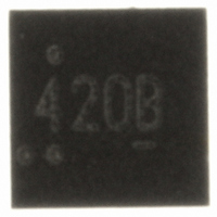
... R Thermal Resistance, Junction-to-Ambient TJA R Thermal Resistance, Junction-to-Ambient TJA Package Marking and Ordering Information Device Marking Device 420 FDMA420NZ ©2009 Fairchild Semiconductor Corporation FDMA420NZ Rev B4 Features „ 30m DS(on) Power Trench „ R =2.5V on special = 40m DS(on) „ Low Profile-0.8mm maximum-in the new package MicroFET 2x2 mm „ ...

Page 2

... TJA drain pins. 2. Pulse Test: Pulse Width < 300 Ps, Duty Cycle < 2.0%. 3. The diode connected between the gate and the source serves only as proection against ESD. No gate overvoltage rating is implied. FDMA420NZ Rev 25°C unless otherwise noted J Test Conditions ...

Page 3

... T , JUNCTION TEMPERATURE J Figure 3. Normalized On Resistance vs Junction Temperature 30 PULSE DURATION = 300 DUTY CYCLE = 2.0%MAX 125 - 0.5 1.0 1 GATE TO SOURCE VOLTAGE (V) GS Figure 5. Transfer Characteristics FDMA420NZ Rev 25°C unless otherwise noted 2. 2.0V GS 1.2 0 Figure 120 160 Figure 4. 100 0.1 0.01 ...

Page 4

... SINGLE PULSE T =MAX RATED 0.01 0 DRAIN TO SOURCE VOLTAGE (V) DS Figure 9. Forward Bias Safe Operating Area 200 100 SINGLE PULSE 1 0 Figure 11. FDMA420NZ Rev 25°C unless otherwise noted J 2000 1000 100 50 0 stics Figure 8. Capacitance vs 6 10us 5 100us 4 1ms 3 10ms 2 100ms 1s 10s Figure 10 ...

Page 5

... Typical Characteristics 2 DUTY CYCLE-DESCENDING ORDER 0.5 0.2 0.1 0.05 0.02 0.01 0.1 SINGLE PULSE 0. Figure 12. FDMA420NZ Rev 25°C unless otherwise noted RECTANGULAR PULSE DURATION(s) Transient Thermal Response Curve NOTES: DUTY FACTOR PEAK TJA TJA 145 C TJA www.fairchildsemi.com ...

Page 6

... Dimensional Outline and Pad Layout FDMA420NZ Rev B4 6 www.fairchildsemi.com ...

Page 7

... PRODUCT STATUS DEFINITIONS Definition of Terms Datasheet Identification Product Status Advance Information Formative / In Design Preliminary First Production No Identification Needed Full Production Obsolete Not In Production FDMA420NZ Rev B4 FPS™ PowerTrench F-PFS™ PowerXS™ ® FRFET Programmable Active Droop™ SM ® Global Power Resource QFET Green FPS™ ...

Related keywords