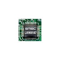
LAN8187-JT SMSC, LAN8187-JT Datasheet - Page 26

LAN8187-JT
Manufacturer Part Number
LAN8187-JT
Description
Ethernet ICs HiPerfrm Ethrnt PHY
Manufacturer
SMSC
Type
MII/RMII Ethernet Transceiverr
Datasheet
1.LAN8187-JT.pdf
(78 pages)
Specifications of LAN8187-JT
Ethernet Connection Type
10 Base-T, 100 Base-TX
Minimum Operating Temperature
0 C
Mounting Style
SMD/SMT
Product
Ethernet Transceivers
Number Of Transceivers
1
Standard Supported
802.3ab
Data Rate
10 MB, 100 MB
Supply Voltage (max)
3.3 V
Supply Voltage (min)
1.8 V
Supply Current (max)
39 mA, 81.6 mA
Maximum Operating Temperature
+ 70 C
Package / Case
TQFP-64
Lead Free Status / RoHS Status
Lead free / RoHS Compliant
Available stocks
Company
Part Number
Manufacturer
Quantity
Price
Company:
Part Number:
LAN8187-JT
Manufacturer:
Standard
Quantity:
1 040
Company:
Part Number:
LAN8187-JT
Manufacturer:
STM
Quantity:
5 362
Part Number:
LAN8187-JT
Manufacturer:
SMSC
Quantity:
20 000
Revision 1.7 (03-04-11)
4.6.2.1
4.6.2.2
4.6.3
The RMII includes 6 interface signals with one of the signals being optional:
Reference Clock
The Reference Clock - CLKIN, is a continuous clock that provides the timing reference for CRS_DV,
RXD[1:0], TX_EN, TXD[1:0], and RX_ER. The Reference Clock is sourced by the MAC or an external
source. Switch implementations may choose to provide REF_CLK as an input or an output depending
on whether they provide a REF_CLK output or rely on an external clock distribution device.
The “Reference Clock” frequency must be 50 MHz +/- 50 ppm with a duty cycle between 40% and
60% inclusive. The SMSC LAN8187/LAN8187i uses the “Reference Clock” as the network clock such
that no buffering is required on the transmit data path. The SMSC LAN8187/LAN8187i will recover the
clock from the incoming data stream, the receiver will account for differences between the local
REF_CLK and the recovered clock through use of sufficient elasticity buffering. The elasticity buffer
does not affect the Inter-Packet Gap (IPG) for received IPGs of 36 bits or greater. To tolerate the clock
variations specified here for Ethernet MTUs, the elasticity buffer shall tolerate a minimum of +/-10 bits.
CRS_DV - Carrier Sense/Receive Data Valid
The CRS_DV is asserted by the LAN8187/LAN8187i when the receive medium is non-idle. CRS_DV
is asserted asynchronously on detection of carrier due to the criteria relevant to the operating mode.
That is, in 10BASE-T mode, when squelch is passed or in 100BASE-X mode when 2 non-contiguous
zeroes in 10 bits are detected, carrier is said to be detected.
Loss of carrier shall result in the deassertion of CRS_DV synchronous to the cycle of REF_CLK which
presents the first di-bit of a nibble onto RXD[1:0] (i.e. CRS_DV is deasserted only on nibble
boundaries). If the LAN8187/LAN8187i has additional bits to be presented on RXD[1:0] following the
initial deassertion of CRS_DV, then the LAN8187/LAN8187i shall assert CRS_DV on cycles of
REF_CLK which present the second di-bit of each nibble and de-assert CRS_DV on cycles of
REF_CLK which present the first di-bit of a nibble. The result is: Starting on nibble boundaries
CRS_DV toggles at 25 MHz in 100Mb/s mode and 2.5 MHz in 10Mb/s mode when CRS ends before
RX_DV (i.e. the FIFO still has bits to transfer when the carrier event ends.) Therefore, the MAC can
accurately recover RX_DV and CRS.
During a false carrier event, CRS_DV shall remain asserted for the duration of carrier activity. The data
on RXD[1:0] is considered valid once CRS_DV is asserted. However, since the assertion of CRS_DV
is asynchronous relative to REF_CLK, the data on RXD[1:0] shall be “00” until proper receive signal
decoding takes place.
MII vs. RMII Configuration
The LAN8187/LAN8187i must be configured to support the MII or RMII bus for connectivity to the MAC.
This configuration is done through the GPO0/RMII pin. To select MII mode, float the GPO0/RMII pin.
To select RMII mode, pull-high with an external resistor (see
Resistors,” on page
18.14 (MIIMODE) is loaded based on the strapping of the GPO0/RMII pin.
Most of the MII and RMII pins are multiplexed.
describes the relationship of the related device pins to what pins are used in MII and RMII mode.
It uses LVCMOS signal levels, compatible with common digital CMOS ASIC processes
transmit data - TXD[1:0]
transmit strobe - TX_EN
receive data - RXD[1:0]
receive error - RX_ER (Optional)
carrier sense - CRS_DV
Reference Clock - CLKIN/XTAL1 (RMII references usually define this signal as REF_CLK)
33) to VDD33. On the rising edge of the internal reset (nreset), the register bit
±15kV ESD Protected MII/RMII 10/100 Ethernet Transceiver with HP Auto-MDIX & flexPWR
DATASHEET
26
Table 4.2, "MII/RMII Signal
Table 4.4, “Boot Strapping Configuration
Mapping", shown below,
SMSC LAN8187/LAN8187i
Datasheet
®
Technology


