FDS6681Z Fairchild Semiconductor, FDS6681Z Datasheet
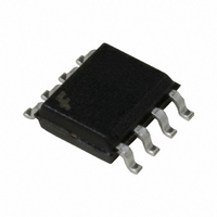
MOSFET P-CH 30V 20A SO-8

FDS6681Z

Manufacturer Part Number
FDS6681Z
Description
MOSFET P-CH 30V 20A SO-8
Manufacturer
Fairchild Semiconductor
Series
PowerTrench®r
Datasheet

Specifications of FDS6681Z

Fet Type
MOSFET P-Channel, Metal Oxide
Fet Feature
Logic Level Gate
Rds On (max) @ Id, Vgs
4.6 mOhm @ 20A, 10V
Drain To Source Voltage (vdss)
30V
Current - Continuous Drain (id) @ 25° C
20A
Vgs(th) (max) @ Id
3V @ 250µA
Gate Charge (qg) @ Vgs
260nC @ 10V
Input Capacitance (ciss) @ Vds
7540pF @ 15V
Power - Max
1W
Mounting Type
Surface Mount
Package / Case
8-SOIC (3.9mm Width)
Configuration
Single Quad Drain Triple Source
Transistor Polarity
P-Channel
Resistance Drain-source Rds (on)
0.0046 Ohm @ 10 V
Forward Transconductance Gfs (max / Min)
79 S
Drain-source Breakdown Voltage
30 V
Gate-source Breakdown Voltage
+/- 25 V
Continuous Drain Current
20 A
Power Dissipation
2500 mW
Maximum Operating Temperature
+ 150 C
Mounting Style
SMD/SMT
Minimum Operating Temperature
- 55 C
Lead Free Status / RoHS Status
Lead free / RoHS Compliant
Other names
FDS6681Z
FDS6681ZTR

Available stocks

Company
Part Number
Manufacturer
Quantity
Price
Part Number:
FDS6681Z
Manufacturer:
Fairchild Semiconductor
Quantity:
375 013
Part Number:
FDS6681Z
Manufacturer:
FAIRCHILD/仙童
Quantity:
20 000
Part Number:
FDS6681Z
0
Company:
Part Number:
FDS6681Z
Quantity:
578
Company:
Part Number:
FDS6681Z
Quantity:
25 000
FDS6681Z
30 Volt P-Channel PowerTrench
General Description
This P-Channel MOSFET is produced using Fairchild
Semiconductor’s advanced PowerTrench
has been especially tailored to minimize the on-state
resistance.
This device is well suited for Power Management and
load switching applications common in Notebook
Computers and Portable Battery Packs.
Absolute Maximum Ratings
Symbol
V
V
P
T
Thermal Characteristics
R
R
Package Marking and Ordering Information
©2005 Fairchild Semiconductor Corporation
I
D
J
DSS
GSS
D
θJA
θJC
Device Marking
, T
STG
FDS6681Z
Drain-Source Voltage
Gate-Source Voltage
Drain Current
Power Dissipation for Single Operation
Operating and Storage Junction Temperature Range
Thermal Resistance, Junction-to-Ambient
Thermal Resistance, Junction-to-Case
D
D
SO-8
D
D
FDS6681Z
Device
– Continuous
– Pulsed
S
Parameter
S
S
®
G
process that
T
A
=25
®
Reel Size
o
C unless otherwise noted
MOSFET
13’’
(Note 1a)
(Note 1a)
(Note 1b)
(Note 1c)
(Note 1a)
(Note 1)
Features
• –20 A, –30 V.
• Extended V
• HBM ESD protection level of 8kV typical (note 3)
• High performance trench technology for extremely
• High power and current handling capability
• Termination is Lead-free and RoHS Compliant
low R
DS(ON)
Tape width
5
6
8
7
GSS
12mm
range (–25V) for battery applications
–55 to +150
R
R
Ratings
DS(ON)
DS(ON)
–105
–30
±25
–20
2.5
1.2
1.0
50
25
= 4.6 mΩ @ V
= 6.5 mΩ @ V
1
4
3
2
June 2005
GS
GS
2500 units
Quantity
FDS6681Z Rev B (W)
= –10 V
= –4.5 V
Units
°C/W
°C/W
°C
W
A
V
V

Related parts for FDS6681Z

FDS6681Z Summary of contents

Page 1

... Reel Size 13’’ June 2005 R = 4.6 mΩ –10 V DS(ON 6.5 mΩ –4.5 V DS(ON) GS range (–25V) for battery applications GSS Ratings Units –30 ±25 –20 –105 2.5 1.2 1.0 °C –55 to +150 °C/W 50 °C/W 25 Tape width Quantity 12mm 2500 units FDS6681Z Rev B ( ...

Page 2

... GEN = –10V V = – – –5V Min Typ Max Units –30 V –26 mV/°C µA –1 µA ±10 –1 –1.8 – mV/°C 3.8 4.6 mΩ 5.2 6.5 5.0 6 7540 pF 1400 pF 1120 660 1060 ns 380 610 ns 185 260 nC 105 150 FDS6681Z Rev B (W) ...

Page 3

... A Test Conditions –2 – /dt = 100 A/µ determined by the user's board design. θCA b) 105°C/W when 2 mounted on a .04 in pad copper Min Typ Max Units –2.1 –0.7 –1.2 (Note 2) 125 94 (Note 2) c) 125°C/W when mounted on a minimum pad. FDS6681Z Rev B ( ...

Page 4

... Figure 6. Body Diode Forward Voltage Variation with Source Current and Temperature. -4.0V -4.5V -5.0V -6.0V -8.0V -10V DRAIN CURRENT ( -10A 125 GATE TO SOURCE VOLTAGE (V) GS Gate-to-Source Voltage 125 -55 C 0.2 0.4 0.6 0 BODY DIODE FORWARD VOLTAGE (V) SD FDS6681Z Rev B (W) 105 10 1.2 ...

Page 5

... Figure 10. Single Pulse Maximum 0.01 0 TIME (sec 1MHz iss C oss DRAIN TO SOURCE VOLTAGE (V) DS SINGLE PULSE R = 125°C/W θ 25° 100 t , TIME (sec) 1 Power Dissipation. R ( θ 125 °C/W θ (t) θ Duty Cycle 100 1000 FDS6681Z Rev B (W) 30 1000 ...

Page 6

... TRADEMARKS The following are registered and unregistered trademarks Fairchild Semiconductor owns or is authorized to use and is not intended exhaustive list of all such trademarks. FAST ® ACEx™ ActiveArray™ FASTr™ Bottomless™ FPS™ Build it Now™ FRFET™ CoolFET™ ...

Related keywords