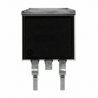
NDB5060L Fairchild Semiconductor, NDB5060L Datasheet

NDB5060L
Specifications of NDB5060L
NDB5060LTR
Available stocks
Related parts for NDB5060L
NDB5060L Summary of contents
Page 1
... NDP5060L / NDB5060L N-Channel Logic Level Enhancement Mode Field Effect Transistor General Description These logic level N-Channel enhancement mode power field effect transistors are produced using Fairchild's proprietary, high cell density, DMOS technology. This very high density process has been especially tailored ...
Page 2
Electrical Characteristics (T = 25°C unless otherwise noted) C Symbol Parameter DRAIN-SOURCE AVALANCHE RATINGS W Single Pulse Drain-Source Avalanche DSS Energy I Maximum Drain-Source Avalanche Current AR OFF CHARACTERISTICS BV Drain-Source Breakdown Voltage DSS I Zero Gate Voltage Drain Current ...
Page 3
Electrical Characteristics (T = 25°C unless otherwise noted) C Symbol Parameter DRAIN-SOURCE DIODE CHARACTERISTICS I Maximum Continuos Drain-Source Diode Forward Current S Maximum Pulsed Drain-Source Diode Forward Current Drain-Source Diode Forward Voltage SD Reverse Recovery Time t ...
Page 4
Typical Electrical Characteristics 10V 6.0 GS 5 DRAIN-SOURCE VOLTAGE (V) DS Figure 1. On-Region Characteristics 13A D 1. ...
Page 5
Typical Electrical Characteristics 1. 250µA D 1.1 1.05 1 0.95 0.9 -50 - JUNCTION TEMPERATURE (°C) J Figure 7. Breakdown Voltage Variation with Temperature . 1500 1000 500 200 ...
Page 6
Typical Electrical Characteristics DRAIN CURRENT (A) D Figure 13. Transconductance Variation with Drain . Current and Temperature 0.5 0.5 0.3 0.2 ...
Page 7
... These larger or intermediate boxes then will b e placed finally inside a labeled shipping box whic h still comes in different sizes depending on the number of units shipped. FSCINT Labe l samp le FAIRCHILD SEMICONDUCTOR CORPORATION HTB:B CBVK741B019 1080 LOT: ...
Page 8
TO-220 Tape and Reel Data and Package Dimensions, continued TO-220 (FS PKG Code 37) 1:1 Scale 1:1 on letter size paper Dimensions shown below are in: inches [millimeters] Part Weight per unit (gram): 1.4378 September 1998, Rev. A ...
Page 9
TO-263AB/D 2 PAK Tape and Reel Data and Package Dimensions 2 TO-263AB/D PAK Packaging Configuration: Figure 1.0 Customized Label 2 TO-263AB/D PAK Packaging Information Standard L86Z Packaging Option (no flow code) Packaging type TNR Rail/Tube Qty per Reel/Tube/Bag 800 45 ...
Page 10
TO-263AB/D 2 PAK Tape and Reel Data and Package Dimensions, continued 2 TO-263AB/D PAK Embossed Carrier Tape Configuration: Figure 3 Pkg type O263AB/ 10.60 15.80 24.0 1. PAK +/-0.10 ...
Page 11
TO-263AB/D 2 PAK Tape and Reel Data and Package Dimensions, continued TO-263AB/D 2 PAK (FS PKG Code 45) Scale 1:1 on letter size paper Dimensions shown below are in: Part Weight per unit (gram): 1.4378 1:1 inches [millimeters] August 1998, ...
Page 12
... TRADEMARKS The following are registered and unregistered trademarks Fairchild Semiconductor owns or is authorized to use and is not intended exhaustive list of all such trademarks. ACEx™ CoolFET™ CROSSVOLT™ CMOS FACT™ FACT Quiet Series™ ® FAST FASTr™ GTO™ ...


