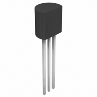
BS270 Fairchild Semiconductor, BS270 Datasheet - Page 4

BS270
Manufacturer Part Number
BS270
Description
MOSFET N-CH 60V 400MA TO-92
Manufacturer
Fairchild Semiconductor
Datasheet
1.BS270.pdf
(10 pages)
Specifications of BS270
Fet Type
MOSFET N-Channel, Metal Oxide
Fet Feature
Logic Level Gate
Rds On (max) @ Id, Vgs
2 Ohm @ 500mA, 10V
Drain To Source Voltage (vdss)
60V
Current - Continuous Drain (id) @ 25° C
400mA
Vgs(th) (max) @ Id
2.5V @ 250µA
Input Capacitance (ciss) @ Vds
50pF @ 25V
Power - Max
625mW
Mounting Type
Through Hole
Package / Case
TO-92-3 (Standard Body), TO-226
Configuration
Single
Transistor Polarity
N-Channel
Resistance Drain-source Rds (on)
2 Ohm @ 10 V
Forward Transconductance Gfs (max / Min)
0.32 S
Drain-source Breakdown Voltage
60 V
Gate-source Breakdown Voltage
+/- 20 V
Continuous Drain Current
0.4 A
Power Dissipation
625 mW
Maximum Operating Temperature
+ 150 C
Mounting Style
Through Hole
Minimum Operating Temperature
- 55 C
Lead Free Status / RoHS Status
Lead free / RoHS Compliant
Gate Charge (qg) @ Vgs
-
Lead Free Status / Rohs Status
Lead free / RoHS Compliant
Available stocks
Company
Part Number
Manufacturer
Quantity
Price
Part Number:
BS270
Manufacturer:
FAIRCHILD/仙童
Quantity:
20 000
Company:
Part Number:
BS270_D74Z
Manufacturer:
Fairchild Semiconductor
Quantity:
40 035
Typical Electrical Characteristics
V
GS
6 0
4 0
2 0
1 0
5
2
1
1.075
1.025
0.975
0.925
Figure 11. Switching Test Circuit.
1
Figure 9. Capacitance Characteristics.
1.05
0.95
Figure 7. Breakdown Voltage Variation
1.1
1
-50
I
R
D
with Temperature.
GEN
f = 1 MHz
V
= 10µA
-25
2
GS
V
DS
= 0V
3
, DRAIN TO SOURCE VOLTAGE (V)
T , JUNCTION TEMPERATURE (°C)
0
J
V
IN
G
5
2 5
5 0
D
S
V
1 0
DD
7 5
R
L
(continued)
DUT
1 0 0
2 0
C iss
C oss
3 0
1 2 5
V
C rss
OUT
1 5 0
5 0
Figure 8. Body Diode Forward Voltage Variation with
Output, V out
Input, V in
0.005
0.001
1 0
Figure 12. Switching Waveforms
Figure 10. Gate Charge Characteristics
Current and Temperature.
0.05
0.01
8
6
4
2
0
0.5
0.1
0
t
2
1
d(on)
0.2
10%
I
D
V
= 5 0 0 m A
T = 125°C
GS
J
0.4
0.4
V
= 0V
SD
t
50%
on
10%
, BODY DIODE FORWARD VOLTAGE (V)
Q
t
0.6
Pulse Width
90%
r
g
0.8
, GATE CHARGE (nC)
25°C
0.8
t
d(off)
V
1.2
DS
50%
-55°C
= 25V
.
1
90%
t
10%
off
90%
1.6
.
1.2
t
Inverted
f
BS270.SAM
1.4
2


