FQD17P06TM Fairchild Semiconductor, FQD17P06TM Datasheet - Page 3
FQD17P06TM
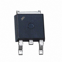
Manufacturer Part Number
FQD17P06TM
Description
MOSFET P-CH 60V 12A DPAK
Manufacturer
Fairchild Semiconductor
Series
QFET™r
Specifications of FQD17P06TM
Fet Type
MOSFET P-Channel, Metal Oxide
Fet Feature
Standard
Rds On (max) @ Id, Vgs
135 mOhm @ 6A, 10V
Drain To Source Voltage (vdss)
60V
Current - Continuous Drain (id) @ 25° C
12A
Vgs(th) (max) @ Id
4V @ 250µA
Gate Charge (qg) @ Vgs
27nC @ 10V
Input Capacitance (ciss) @ Vds
900pF @ 25V
Power - Max
2.5W
Mounting Type
Surface Mount
Package / Case
DPak, TO-252 (2 leads+tab), SC-63
Configuration
Single
Transistor Polarity
P-Channel
Resistance Drain-source Rds (on)
0.135 Ohms
Forward Transconductance Gfs (max / Min)
8.7 S
Drain-source Breakdown Voltage
- 60 V
Gate-source Breakdown Voltage
+/- 25 V
Continuous Drain Current
- 12 A
Power Dissipation
2.5 W
Maximum Operating Temperature
+ 150 C
Mounting Style
SMD/SMT
Minimum Operating Temperature
- 55 C
Lead Free Status / RoHS Status
Lead free / RoHS Compliant
Other names
FQD17P06TM
Available stocks
Company
Part Number
Manufacturer
Quantity
Price
Company:

Part Number:
FQD17P06TM
Manufacturer:
FSC
Quantity:
30 000


©2009 Fairchild Semiconductor Corporation
Typical Characteristics
2000
1800
1600
1400
1200
1000
0.40
0.36
0.32
0.28
0.24
0.20
0.16
0.12
0.08
0.04
0.00
800
600
400
200
10
10
1
0
0
10
10
0
Figure 5. Capacitance Characteristics
-1
Figure 3. On-Resistance Variation vs.
-1
Top :
Bottom : - 4.5 V
Figure 1. On-Region Characteristics
Drain Current and Gate Voltage
- 15.0 V
- 10.0 V
- 8.0 V
- 7.0 V
- 6.0 V
- 5.5 V
- 5.0 V
V
10
GS
-V
V
DS
DS
20
, Drain-Source Voltage [V]
, Drain-Source Voltage [V]
-I
D
10
, Drain Current [A]
C
C
10
C
0
iss
rss
oss
0
V
GS
= - 20V
30
V
GS
= - 10V
40
C
C
C
iss
oss
rss
※ Notes :
= C
= C
= C
1. 250μ s Pulse Test
2. T
10
※ Note : T
gs
gd
ds
1
C
+ C
+ C
= 25℃
※ Notes :
10
gd
gd
1. V
2. f = 1 MHz
1
50
(C
J
ds
GS
= 25℃
= shorted)
= 0 V
60
10
10
10
10
10
10
12
10
8
6
4
2
0
-1
-1
1
0
1
0
0.0
0
2
Figure 6. Gate Charge Characteristics
Figure 4. Body Diode Forward Voltage
25℃
0.2
Figure 2. Transfer Characteristics
150℃
Variation vs. Source Current
150℃
0.4
4
0.6
4
-V
-V
Q
SD
and Temperature
GS
-55℃
25℃
G
0.8
8
, Source-Drain Voltage [V]
, Total Gate Charge [nC]
, Gate-Source Voltage [V]
V
1.0
DS
V
DS
= -48V
= -30V
1.2
12
6
1.4
1.6
16
※ Notes :
※ Notes :
1. V
2. 250μ s Pulse Test
1. V
2. 250μ s Pulse Test
1.8
※ Note : I
8
DS
GS
= -30V
= 0V
2.0
20
D
= -17 A
2.2
Rev. A3. Januaary 2009
2.4
10
24
Related parts for FQD17P06TM
Image
Part Number
Description
Manufacturer
Datasheet
Request
R

Part Number:
Description:
Fairchild Semiconductor [IGBT MODULE]
Manufacturer:
Fairchild Semiconductor
Datasheet:

Part Number:
Description:
Discrete Semiconductor Modules
Manufacturer:
Fairchild Semiconductor
Part Number:
Description:
Discrete Semiconductor Modules
Manufacturer:
Fairchild Semiconductor
Part Number:
Description:
This N-Channel MOSFET is produced using Fairchild Semiconductor’s advanced Power Trench® process
Manufacturer:
Fairchild Semiconductor
Datasheet:
Part Number:
Description:
This N-Channel MOSFET is produced using Fairchild Semiconductor’s advanced Power Trench® process
Manufacturer:
Fairchild Semiconductor
Datasheet:
Part Number:
Description:
This N-Channel MOSFET is produced using Fairchild Semiconductor’s advanced PowerTrench® process
Manufacturer:
Fairchild Semiconductor
Datasheet:
Part Number:
Description:
This N-Channel MOSFET is produced using Fairchild Semiconductor’s advanced PowerTrench® process
Manufacturer:
Fairchild Semiconductor
Datasheet:
Part Number:
Description:
This N-Channel MOSFET is produced using Fairchild Semiconductor’s advanced Power Trench® process
Manufacturer:
Fairchild Semiconductor
Datasheet:
Part Number:
Description:
This N-Channel logic Level MOSFETs are produced using Fairchild Semiconductor‘s advanced Power Trench® process that has been special tailored to minimize the on-state resistance and yet maintain superior switching performance
Manufacturer:
Fairchild Semiconductor
Datasheet:
Part Number:
Description:
This N-Channel MOSFET is produced using Fairchild Semiconductor’s advanced Power Trench® process
Manufacturer:
Fairchild Semiconductor
Datasheet:
Part Number:
Description:
This N-Channel SyncFET™ is produced using Fairchild Semiconductor’s advanced PowerTrench® process
Manufacturer:
Fairchild Semiconductor
Datasheet:
Part Number:
Description:
This N-Channel SyncFET™ is produced using Fairchild Semiconductor’s advanced PowerTrench® process
Manufacturer:
Fairchild Semiconductor
Datasheet:
Part Number:
Description:
This N-Channel SyncFET™ is produced using Fairchild Semiconductor’s advanced PowerTrench® process
Manufacturer:
Fairchild Semiconductor
Datasheet:
Part Number:
Description:
This N-Channel logic Level MOSFETs are produced using Fairchild Semiconductor‘s advanced Power Trench® process that has been special tailored to minimize the on-state resistance and yet maintain superior switching performance
Manufacturer:
Fairchild Semiconductor
Datasheet:
Part Number:
Description:
This N-Channel MOSFET is produced using Fairchild Semiconductor’s advanced Power Trench® process that has been especially tailored to minimize the on-state resistance and yet maintain superior switching performance
Manufacturer:
Fairchild Semiconductor
Datasheet: