FDB8880 Fairchild Semiconductor, FDB8880 Datasheet
FDB8880
Specifications of FDB8880
Available stocks


Related parts for FDB8880


FDB8880 Summary of contents
Page 1
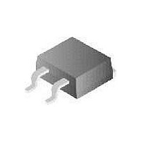
... RoHS Complicant DRAIN (FLANGE) GATE SOURCE TO-263AB FDB SERIES ©2008 Fairchild Semiconductor Corporation FDP8880 / FDB8880 Rev. A1 ® MOSFET General Description This N-Channel MOSFET has been designed specifically to = 40A improve the overall efficiency of DC/DC converters using either synchronous or conventional switching PWM controllers. It has been optimized for low gate charge, low r and fast switching speed ...
Page 2
... Drain to Source Breakdown Voltage VDSS I Zero Gate Voltage Drain Current DSS I Gate to Source Leakage Current GSS On Characteristics V Gate to Source Threshold Voltage GS(TH) r Drain to Source On Resistance DS(ON) ©2008 Fairchild Semiconductor Corporation FDP8880 / FDB8880 Rev 25°C unless otherwise noted C Parameter 10V 4.5V 10V, with ...
Page 3
... Turn-Off Time OFF Drain-Source Diode Characteristics V Source to Drain Diode Voltage SD t Reverse Recovery Time rr Q Reverse Recovered Charge RR Notes: 1: Starting T = 25° 34uH 43A,Vdd = 27V, Vgs = 10V Pulse width = 100s. 3 ©2008 Fairchild Semiconductor Corporation FDP8880 / FDB8880 Rev 15V 0V 1MHz V = 0.5V 1MHz 10V ...
Page 4
... SINGLE PULSE 0. Figure 3. Normalized Maximum Transient Thermal Impedance 600 TRANSCONDUCTANCE MAY LIMIT CURRENT IN THIS REGION 4.5V GS 100 ©2008 Fairchild Semiconductor Corporation FDP8880 / FDB8880 Rev 25°C unless otherwise noted 150 175 125 Figure 2. Maximum Continuous Drain Current RECTANGULAR PULSE DURATION (s) = 10V GS -3 ...
Page 5
... GATE TO SOURCE VOLTAGE (V) GS Figure 7. Transfer Characteristics 54A GATE TO SOURCE VOLTAGE (V) GS Figure 9. Drain to Source On Resistance vs Gate Voltage and Drain Current ©2008 Fairchild Semiconductor Corporation FDP8880 / FDB8880 Rev 25°C unless otherwise noted C 500 100 100 s 1ms 10 10ms DC 1 0.001 10 40 NOTE: Refer to Fairchild Application Notes AN7514 and AN7515 Figure 6 ...
Page 6
... Figure 11. Normalized Gate Threshold Voltage vs Junction Temperature 2000 1000 C C RSS 0V 1MHz GS 100 0 DRAIN TO SOURCE VOLTAGE (V) DS Figure 13. Capacitance vs Drain to Source Voltage ©2008 Fairchild Semiconductor Corporation FDP8880 / FDB8880 Rev 25°C unless otherwise noted C 1 250 1.0 0.9 -80 80 120 160 200 o C) Figure 12 ...
Page 7
... Test Circuits and Waveforms VARY t TO OBTAIN P R REQUIRED PEAK Figure 15. Unclamped Energy Test Circuit g(REF) Figure 17. Gate Charge Test Circuit Figure 19. Switching Time Test Circuit ©2008 Fairchild Semiconductor Corporation FDP8880 / FDB8880 Rev DUT 0.01 Figure 16. Unclamped Energy Waveforms gs2 DUT ...
Page 8
... Note: For further discussion of the PSPICE model, consult A New PSPICE Sub-Circuit for the Power MOSFET Featuring Global Temperature Options; IEEE Power Electronics Specialist Conference Records, 1991, written by William J. Hepp and C. Frank Wheatley. ©2008 Fairchild Semiconductor Corporation FDP8880 / FDB8880 Rev. A1 DPLCAP 5 10 ...
Page 9
... Fairchild Semiconductor Corporation FDP8880 / FDB8880 Rev. A1 DPLCAP 10 RSLC2 - 6 ESG 8 EVTHRES ...
Page 10
... Fairchild Semiconductor Corporation FDP8880 / FDB8880 Rev. A1 JUNCTION th RTHERM1 6 RTHERM2 5 RTHERM3 4 RTHERM4 3 RTHERM5 ...
Page 11
... Product Status Advance Information Formative or In Design Preliminary First Production No Identification Needed Full Production Obsolete Not In Production @2008 Fairchild Semiconductor Corporation FDP8880 / FDB8880 Rev.A1 FPS™ PDP-SPM™ F-PFS™ Power-SPM™ ® FRFET PowerTrench Global Power Resource SM Programmable Active Droop™ ...