FDD6680AS Fairchild Semiconductor, FDD6680AS Datasheet
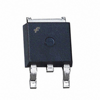
MOSFET N-CH 30V 55A DPAK

FDD6680AS

Manufacturer Part Number
FDD6680AS
Description
MOSFET N-CH 30V 55A DPAK
Manufacturer
Fairchild Semiconductor
Series
PowerTrench®r
Datasheet

Specifications of FDD6680AS

Fet Type
MOSFET N-Channel, Metal Oxide
Fet Feature
Logic Level Gate
Rds On (max) @ Id, Vgs
10.5 mOhm @ 12.5A, 10V
Drain To Source Voltage (vdss)
30V
Current - Continuous Drain (id) @ 25° C
55A
Vgs(th) (max) @ Id
3V @ 1mA
Gate Charge (qg) @ Vgs
29nC @ 15V
Input Capacitance (ciss) @ Vds
1200pF @ 15V
Power - Max
1.3W
Mounting Type
Surface Mount
Package / Case
DPak, TO-252 (2 leads+tab), SC-63
Configuration
Single
Transistor Polarity
N-Channel
Resistance Drain-source Rds (on)
0.0105 Ohm @ 10 V
Forward Transconductance Gfs (max / Min)
44 S
Drain-source Breakdown Voltage
30 V
Gate-source Breakdown Voltage
+/- 20 V
Continuous Drain Current
55 A
Power Dissipation
60000 mW
Maximum Operating Temperature
+ 150 C
Mounting Style
SMD/SMT
Minimum Operating Temperature
- 55 C
Continuous Drain Current Id
55A
Drain Source Voltage Vds
30V
On Resistance Rds(on)
10.5mohm
Rds(on) Test Voltage Vgs
10V
Threshold Voltage Vgs Typ
1.4V
Rohs Compliant
Yes
Lead Free Status / RoHS Status
Lead free / RoHS Compliant

Available stocks

Company
Part Number
Manufacturer
Quantity
Price
Part Number:
FDD6680AS
Manufacturer:
FAIRCHILD
Quantity:
30 000
FDD6680AS
30V N-Channel PowerTrench
General Description
The FDD6680AS is designed to replace a single
MOSFET and Schottky diode in synchronous DC:DC
power supplies.
maximize power conversion efficiency, providing a low
R
includes an integrated Schottky diode using Fairchild’s
monolithic SyncFET technology.
the
synchronous rectifier is indistinguishable from the
performance of the FDD6680A in parallel with a
Schottky diode.
Applications
• DC/DC converter
• Low side notebook
©2008 Fairchild Semiconductor Corporation
DS(ON)
Absolute Maximum Ratings
Symbol
V
V
I
P
T
Thermal Characteristics
R
R
R
Package Marking and Ordering Information
D
J
Device Marking
DSS
GSS
D
θJC
θJA
θJA
, T
FDD6680AS
FDD6680AS
STG
and low gate charge.
Drain-Source Voltage
Gate-Source Voltage
Drain Current
Power Dissipation
Operating and Storage Junction Temperature Range
Thermal Resistance, Junction-to-Case
Thermal Resistance, Junction-to-Ambient
This 30V MOSFET is designed to
G
as
S
the
FDD6680AS
low-side
– Continuous
– Pulsed
TO-252
Device
The performance of
The FDD6680AS
Parameter
switch
D
®
SyncFET
T
in
A
=25
o
a
C unless otherwise noted
Reel Size
(Note 1a)
(Note 1a)
(Note 1b)
(Note 1a)
(Note 1b)
(Note 3)
(Note 1)
(Note 1)
13’’
Features
• 55 A, 30 V
• Includes SyncFET Schottky body diode
• Low gate charge (21nC typical)
• High performance trench technology for extremely
• High power and current handling capability
.
low R
DS(ON)
R
R
DS(ON)
DS(ON)
G
Tape width
–55 to +150
16mm
max= 10.5 mΩ @ V
Ratings
max= 13.0 mΩ @ V
±20
100
3.1
1.3
2.1
30
55
60
40
96
D
S
April 2008
2500 units
FDD6680AS Rev A1(X)
Quantity
GS
GS
= 10 V
= 4.5 V
Unit
°C/W
°C/W
°C/W
°C
W
s
V
V
A
tm

Related parts for FDD6680AS

FDD6680AS Summary of contents

Page 1

... FDD6680AS 30V N-Channel PowerTrench General Description The FDD6680AS is designed to replace a single MOSFET and Schottky diode in synchronous DC:DC power supplies. This 30V MOSFET is designed to maximize power conversion efficiency, providing a low R and low gate charge. The FDD6680AS DS(ON) includes an integrated Schottky diode using Fairchild’s monolithic SyncFET technology ...

Page 2

... R GS GEN Ω 4 GEN 12 4.4 A (Note (Note 12.5A 300 A/µs (Note Min Typ Max Units 54 205 mJ 13 mV/°C µA 500 ±100 –3 mV/°C 8.6 10.5 mΩ 10.3 13.0 12.5 16 1200 pF 350 pF 120 pF Ω 1 4.4 A 0.5 0 FDD6680AS Rev A1 (X) ...

Page 3

... T = 25°C and T = 25°C unless otherwise noted A is determined by the user's board design. θCA = 40°C/W when mounted on a θJA 2 1in pad copper D = 10V. Package current limitation is 21A and V DS(on) J(max 96°C/W when mounted θ minimum pad. FDD6680AS Rev A1 (X) ...

Page 4

... Figure 6. Body Diode Forward Voltage Variation with Source Current and Temperature. 3.5V 4.0V 4.5V 5.0V 6.0V 10V DRAIN CURRENT ( 6. 125 = GATE TO SOURCE VOLTAGE ( Gate-to-Source Voltage 125 -55 C 0.2 0.4 0.6 0 BODY DIODE FORWARD VOLTAGE (V) SD FDD6680AS Rev A1 (X) 100 10 1 ...

Page 5

... Figure 10. Single Pulse Maximum 0.01 0 TIME (sec 1MHz iss C oss rss DRAIN TO SOURCE VOLTAGE (V) DS SINGLE PULSE R = 96°C/W θ 25°C A 0.01 0 100 t , TIME (sec) 1 Power Dissipation. R ( θJA θ °C/W θJA P( (t) θ Duty Cycle 100 1000 FDD6680AS Rev A1 (X) 30 1000 ...

Page 6

... Schottky diode in parallel with a MOSFET. Figure 12 shows the reverse recovery characteristic of the FDD6680AS. 10nS/div Figure 12. FDD6680AS SyncFET body diode reverse recovery characteris For comparison purposes, Figure 13 shows the reverse recovery characteristics of the body diode of an equivalent size MOSFET produced without SyncFET (FDD6680) ...

Page 7

... Pulse Width ≤ 1µs Duty Cycle ≤ 0.1% Figure 16. Switching Time Test Circuit + Figure 13. Unclamped Inductive Waveforms + 10V DUT Charge, (nC) Figure 15. Gate Charge Waveform d(ON 90% + DUT 50% 10% 0V Figure 17. Switching Time Waveforms BV DSS G(TOT OFF t d(OFF 90% 10% 10% 90% 50% Pulse Width FDD6680AS Rev A1 (X) ...

Page 8

... Fairchild Semiconductor. The datasheet is for reference information only. The Power Franchise ® tm TinyBoost™ TinyBuck™ ® TinyLogic TINYOPTO™ TinyPower™ TinyPWM™ TinyWire™ µSerDes™ ® UHC Ultra FRFET™ UniFET™ VCX™ VisualMax™ ® Definition FDD6680AS Rev A1(X) ® Rev. I34 ...

Related keywords