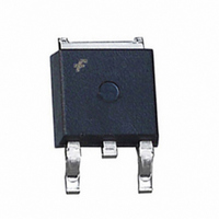
FDD2582 Fairchild Semiconductor, FDD2582 Datasheet

FDD2582
Specifications of FDD2582
Available stocks
Related parts for FDD2582
FDD2582 Summary of contents
Page 1
... JC R Thermal Resistance Junction to Ambient TO-252 JA R Thermal Resistance Junction to Ambient TO-252, 1in JA ©2010 Fairchild Semiconductor Corporation FDD2582 Rev.B1 ® MOSFET Applications = 7A • DC/DC converters and Off-Line UPS D • Distributed Power Architectures and VRMs • Primary Switch for 24V and 48V Systems • ...
Page 2
... Drain-Source Diode Characteristics V Source to Drain Diode Voltage SD t Reverse Recovery Time rr Q Reverse Recovered Charge RR Notes: 1: Starting T = 25° 1.17 mH 10A ©2010 Fairchild Semiconductor Corporation FDD2582 Rev.B1 Package Reel Size TO-252AA 330mm T = 25°C unless otherwise noted C Test Conditions I = 250 120V DS ...
Page 3
... SINGLE PULSE 0. Figure 3. Normalized Maximum Transient Thermal Impedance 300 TRANSCONDUCTANCE MAY LIMIT CURRENT IN THIS REGION 100 V = 10V ©2010 Fairchild Semiconductor Corporation FDD2582 Rev. 25°C unless otherwise noted 150 175 125 Figure 2. Maximum Continuous Drain Current RECTANGULAR PULSE DURATION ( ...
Page 4
... PULSE DURATION = 80 s DUTY CYCLE = 0.5% MAX 10V DRAIN CURRENT (A) D Figure 9. Drain to Source On Resistance vs Drain Current ©2010 Fairchild Semiconductor Corporation FDD2582 Rev. 25°C unless otherwise noted C 100 100 1ms 10 10ms DC 1 100 300 0.001 NOTE: Refer to Fairchild Application Notes AN7514 and AN7515 Figure 6 ...
Page 5
... OSS RSS GD 100 1MHz DRAIN TO SOURCE VOLTAGE (V) DS Figure 13. Capacitance vs Drain to Source Voltage ©2010 Fairchild Semiconductor Corporation FDD2582 Rev. 25°C unless otherwise noted C 1 250 1.1 1.0 0.9 -80 80 120 160 200 o C) Figure 12. Normalized Drain to Source Breakdown Voltage vs Junction Temperature ...
Page 6
... Test Circuits and Waveforms VARY t TO OBTAIN P REQUIRED PEAK Figure 15. Unclamped Energy Test Circuit g(REF) Figure 17. Gate Charge Test Circuit Figure 19. Switching Time Test Circuit ©2010 Fairchild Semiconductor Corporation FDD2582 Rev. DUT 0.01 Figure 16. Unclamped Energy Waveforms DUT g(TH g(REF) 0 Figure 18. Gate Charge Waveforms ...
Page 7
... The area, in square inches or square centimeters is the top copper area including the gate and source pads. 23.84 33.32 + ------------------------------------ - 0.268 + Area 154 33.32 + --------------------------------- - 1.73 + Area ©2010 Fairchild Semiconductor Corporation FDD2582 Rev.B1 , and the JM 125 , application’s ambient 100 never exceeded (EQ 0.01 (0.0645 Figure 21 ...
Page 8
... PSPICE Electrical Model .SUBCKT FDD2582 rev July 2002 4e- 4.6e-10 Cin 6 8 1.24e-9 Dbody 7 5 DbodyMOD Dbreak 5 11 DbreakMOD Dplcap 10 5 DplcapMOD Ebreak 160.4 Eds Egs Esg Evthres Evtemp GATE Lgate 1 9 4.88e-9 Ldrain 2 5 1.0e-9 Lsource 3 7 2.24e-9 RLgate 1 9 48.8 RLdrain RLsource ...
Page 9
... SABER Electrical Model REV July 2002 ttemplate FDD2582 n2,n1,n3 electrical n2,n1,n3 { var i iscl dp..model dbodymod = (isl=2.3e-12,rs=5.3e-3,trs1=2.2e-3,trs2=4.5e-7,cjo=8.8e-10,m=0.64,tt=3.8e-8,xti=4.2) dp..model dbreakmod = (rs=0.4,trs1=1.4e-3,trs2=-5.0e-5) dp..model dplcapmod = (cjo=2.75e-10,isl=10.0e-30,nl=10,m=0.67) m..model mmedmod = (type=_n,vto=3.76,kp=2.7,is=1e-30, tox=1) m..model mstrongmod = (type=_n,vto=4.25,kp=30,is=1e-30, tox=1) m..model mweakmod = (type=_n,vto=3.2,kp=0.068,is=1e-30, tox=1,rs=0.1) sw_vcsp..model s1amod = (ron=1e-5,roff=0.1,von=-5.0,voff=-2.0) sw_vcsp ...
Page 10
... RTHERM1 TH 6 3.3e-2 RTHERM2 6 5 7.9e-2 RTHERM3 5 4 9.5e-2 RTHERM4 4 3 1.4e-1 RTHERM5 3 2 2.9e-1 RTHERM6 2 TL 6.7e-1 SABER Thermal Model SABER thermal model FDD2582 template thermal_model th tl thermal_c th ctherm.ctherm1 th 6 =1.6e-3 ctherm.ctherm2 6 5 =4.5e-3 ctherm.ctherm3 5 4 =5.0e-3 ctherm.ctherm4 4 3 =8.0e-3 ctherm ...
Page 11
... Datasheet Identification Product Status Advance Information Formative / In Design Preliminary First Production No Identification Needed Full Production Obsolete Not In Production ©2010 Fairchild Semiconductor Corporation FDD2582 Rev.B1 ® PowerTrench ® PowerXS™ SM Programmable Active Droop™ ® QFET QS™ Quiet Series™ RapidConfigure™ ...


