NDT456P Fairchild Semiconductor, NDT456P Datasheet
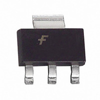
MOSFET P-CH 30V 7.5A SOT-223-4

NDT456P

Manufacturer Part Number
NDT456P
Description
MOSFET P-CH 30V 7.5A SOT-223-4
Manufacturer
Fairchild Semiconductor
Datasheet

Specifications of NDT456P

Fet Type
MOSFET P-Channel, Metal Oxide
Fet Feature
Logic Level Gate
Rds On (max) @ Id, Vgs
30 mOhm @ 7.5A, 10V
Drain To Source Voltage (vdss)
30V
Current - Continuous Drain (id) @ 25° C
7.5A
Vgs(th) (max) @ Id
3V @ 250µA
Gate Charge (qg) @ Vgs
67nC @ 10V
Input Capacitance (ciss) @ Vds
1440pF @ 15V
Power - Max
1.1W
Mounting Type
Surface Mount
Package / Case
SOT-223 (3 leads + Tab), SC-73, TO-261
Configuration
Single Dual Drain
Transistor Polarity
P-Channel
Resistance Drain-source Rds (on)
0.03 Ohm @ 10 V
Forward Transconductance Gfs (max / Min)
13 S
Drain-source Breakdown Voltage
30 V
Gate-source Breakdown Voltage
+/- 20 V
Continuous Drain Current
7.5 A
Power Dissipation
3000 mW
Maximum Operating Temperature
+ 150 C
Mounting Style
SMD/SMT
Minimum Operating Temperature
- 65 C
Continuous Drain Current Id
7.3A
Drain Source Voltage Vds
30V
On Resistance Rds(on)
35mohm
Rds(on) Test Voltage Vgs
-10V
Threshold Voltage Vgs Typ
1.5V
Rohs Compliant
Yes
Lead Free Status / RoHS Status
Lead free / RoHS Compliant
Other names
NDT456PTR

Available stocks

Company
Part Number
Manufacturer
Quantity
Price
Part Number:
NDT456P
Manufacturer:
NDK
Quantity:
40 000
Part Number:
NDT456P
Manufacturer:
FSC
Quantity:
17 500
Part Number:
NDT456P
Manufacturer:
FAIRCHILD/仙童
Quantity:
20 000
Absolute Maximum Ratings
______________________________________________________________________________
Symbol
V
V
I
P
T
THERMAL CHARACTERISTICS
R
R
© 1998 Fairchild Semiconductor Corporation
D
J
DSS
GSS
D
NDT456P
P-Channel Enhancement Mode Field Effect Transistor
General Description
,T
Power SOT P-Channel enhancement mode power field
effect
proprietary, high cell density, DMOS technology. This
very high density process is especially tailored to
minimize on-state resistance and provide superior
switching performance. These devices are particularly
suited for low voltage applications such as notebook
computer power management, battery powered circuits,
and DC motor control.
JA
JC
STG
transistors
Parameter
Drain-Source Voltage
Gate-Source Voltage
Drain Current
Maximum Power Dissipation
Operating and Storage Temperature Range
Thermal Resistance, Junction-to-Ambient
Thermal Resistance, Junction-to-Case
are
- Continuous
- Pulsed
produced
T
G
using
A
= 25°C unless otherwise noted
D
D
Fairchild's
(Note 1c)
(Note 1)
(Note 1a)
(Note 1b)
(Note 1a)
(Note 1a)
S
Features
-7.5 A, -30 V. R
High density cell design for extremely low R
High power and current handling capability in a widely
used surface mount package.
R
-65 to 150
NDT456P
DS(ON)
DS(ON)
±7.5
±20
±20
-30
1.3
1.1
42
12
3
= 0.045
= 0.030
@ V
@ V
G
GS
GS
December 1998
= -4.5 V.
= -10 V
D
DS(ON)
NDT456P Rev. F
.
S
°C/W
°C/W
Units
°C
W
V
V
A

Related parts for NDT456P

NDT456P Summary of contents

Page 1

... High power and current handling capability in a widely used surface mount package 25°C unless otherwise noted A (Note 1a) (Note 1a) (Note 1b) (Note 1c) (Note 1a) (Note 1) December 1998 = 0.030 @ V = -10 V DS(ON 0.045 @ V = -4.5 V. DS(ON DS(ON NDT456P Units -30 V ±20 V ±7.5 A ± 1.3 1.1 -65 to 150 °C 42 °C/W 12 °C/W NDT456P Rev. F ...

Page 2

... - - 1.0 MHz GEN GEN Min Typ Max - 55°C -10 J 100 -100 -1 -1 125°C -0.5 -1.1 -2.6 J 0.026 0. 125°C 0.035 0.054 J 0.041 0.045 -20 -10 13 1440 905 355 120 70 130 70 130 NDT456P Rev. F Units V µA µ ...

Page 3

... defined by users. For general reference: Applications on 4.5"x5" FR-4 PCB under still air environment pad of 2oz copper. 1b Min Typ Max Units -2 0.85 -1.2 V 140 ns 1c NDT456P Rev. F ...

Page 4

... Figure 6. Gate Threshold Variation with =-3.5V -4.0 -4.5 -5.0 -7 -12 - DRAIN CURRENT (A) D Voltage and Drain Current. = -10V T = 125°C J 25°C -55° -12 - DRAIN CURRENT (A) D Current and Temperature 250µ JUNCTION TEM PERATURE (°C) J Temperature. -10 -20 - NDT456P Rev. F ...

Page 5

... Figure 10. Gate Charge Characteristics. t d(on OUT V OUT DUT V IN 10% . Figure 12. Switching Waveforms 125°C J 25°C -55°C 0.2 0.4 0.6 0 BODY DIODE FORWARD VOLTAGE ( with Current and Temperature -10V -20V GATE CHARGE (nC off t t d(off) r 90% 90% 10% 10% 90% 50% 50% PULSE W IDTH 1 INVERTED NDT456P Rev. F ...

Page 6

... SINGLE PULSE 0.1 4.5"x5" FR-4 Board See Note 0.03 A Still Air V = -10V GS 0.01 0.1 0.2 0 Figure 16. Maximum Safe Operating Area TIM E (sec) 1 4.5"x5" FR-4 Board Still Air COPPER ING PAD AREA ( -10V = 25°C 0 DRAIN-SOURCE VOLTAGE ( ( See Note P ( Duty Cycle NDT456P Rev. F ...

Page 7

... TRADEMARKS The following are registered and unregistered trademarks Fairchild Semiconductor owns or is authorized to use and is not intended exhaustive list of all such trademarks. ACEx™ CoolFET™ CROSSVOLT™ CMOS FACT™ FACT Quiet Series™ ® FAST FASTr™ GTO™ ...

Related keywords