NDB6030PL Fairchild Semiconductor, NDB6030PL Datasheet
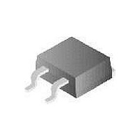
MOSFET P-CH 30V 30A D2PAK

NDB6030PL

Manufacturer Part Number
NDB6030PL
Description
MOSFET P-CH 30V 30A D2PAK
Manufacturer
Fairchild Semiconductor
Datasheet

Specifications of NDB6030PL

Fet Type
MOSFET P-Channel, Metal Oxide
Fet Feature
Logic Level Gate
Rds On (max) @ Id, Vgs
25 mOhm @ 19A, 10V
Drain To Source Voltage (vdss)
30V
Current - Continuous Drain (id) @ 25° C
30A
Vgs(th) (max) @ Id
2V @ 250µA
Gate Charge (qg) @ Vgs
36nC @ 5V
Input Capacitance (ciss) @ Vds
1570pF @ 15V
Power - Max
75W
Mounting Type
Surface Mount
Package / Case
D²Pak, TO-263 (2 leads + tab)
Configuration
Single
Transistor Polarity
P-Channel
Resistance Drain-source Rds (on)
0.037 Ohms
Drain-source Breakdown Voltage
- 30 V
Gate-source Breakdown Voltage
+/- 16 V
Continuous Drain Current
- 30 A
Power Dissipation
75 W
Maximum Operating Temperature
+ 175 C
Mounting Style
SMD/SMT
Minimum Operating Temperature
- 65 C
Lead Free Status / RoHS Status
Lead free / RoHS Compliant

Available stocks

Company
Part Number
Manufacturer
Quantity
Price
Part Number:
NDB6030PL
Manufacturer:
SEMIKRON
Quantity:
200
Part Number:
NDB6030PL
Manufacturer:
FAIRCHILD/仙童
Quantity:
20 000
Absolute Maximum Ratings
________________________________________________________________________________
Symbol
V
V
I
P
T
T
T
THERMAL CHARACTERISTICS
R
R
© 1997 Fairchild Semiconductor Corporation
General Description
D
NDP6030PL / NDB6030PL
P-Channel Logic Level Enhancement Mode Field Effect Transistor
These P-Channel logic level enhancement mode power field
effect transistors are produced using Fairchild's proprietary,
high cell density, DMOS technology. This very high density
process is especially tailored to minimize on-state resistance.
These devices are particularly suited for low voltage
applications such as DC/DC converters and high efficiency
switching circuits where fast switching, low in-line power loss,
and resistance to transients are needed.
J
L
J
DSS
GSS
D
,T
,T
JC
JA
STG
STG
Parameter
Drain-Source Voltage
Gate-Source Voltage - Continuous
Drain Current
Total Power Dissipation @ T
Operating and Storage Temperature Range
Maximum lead temperature for soldering purposes,
1/8" from case for 5 seconds
Operating and Storage Temperature Range
Thermal Resistance, Junction-to-Case
Thermal Resistance, Junction-to-Ambient
- Continuous
- Pulsed
Derate above 25°C
C
= 25°C
T
C
= 25°C unless otherwise noted
Features
NDP6030PL
-30 A, -30 V. R
Critical DC electrical parameters specified at elevated
temperature.
Rugged internal source-drain diode can eliminate the need
for an external Zener diode transient suppressor.
High density cell design for extremely low R
175°C maximum junction temperature rating.
R
-65 to 175
-65 to 175
DS(ON)
DS(ON)
62.5
±16
275
-30
-30
-90
0.5
75
2
= 0.025
= 0.042
G
NDB6030PL
@ V
@ V
GS
GS
= -10 V
= -4.5 V
S
D
DS(ON)
.
NDP6030PL Rev.B1
June 1997
.
Units
°C/W
°C/W
W
°C
°C
°C
V
V
A

Related parts for NDB6030PL

NDB6030PL Summary of contents

Page 1

... NDP6030PL / NDB6030PL P-Channel Logic Level Enhancement Mode Field Effect Transistor General Description These P-Channel logic level enhancement mode power field effect transistors are produced using Fairchild's proprietary, high cell density, DMOS technology. This very high density process is especially tailored to minimize on-state resistance. ...

Page 2

Electrical Characteristics (T = 25°C unless otherwise noted) C Symbol Parameter OFF CHARACTERISTICS BV Drain-Source Breakdown Voltage DSS Breakdown Voltage Temp. Coefficient DSS J Zero Gate Voltage Drain Current I DSS Gate - Body Leakage, Forward I ...

Page 3

Typical Electrical Characteristics -10V -7.0 GS -6.0 -5.0 -4 DRAIN-SOURCE VOLTAGE (V) DS Figure 1. On-Region Characteristics. 1 -15A D 1 -4.5V GS ...

Page 4

Typical Electrical Characteristics -30A GATE CHARGE (nC) g Figure 7. Gate Charge Characteristics. 150 100 -4. ...

Related keywords