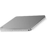
TMC2192KHC Fairchild Semiconductor, TMC2192KHC Datasheet - Page 5

TMC2192KHC
Manufacturer Part Number
TMC2192KHC
Description
Video ICs
Manufacturer
Fairchild Semiconductor
Type
Encoderr
Datasheet
1.TMC2192KHC.pdf
(69 pages)
Specifications of TMC2192KHC
Operating Supply Voltage
- 0.5 V to + 7 V
Supply Current
375 mA
Maximum Operating Temperature
70 C
Package / Case
MQFP-100
Minimum Operating Temperature
0 C
Mounting Style
SMD/SMT
Lead Free Status / RoHS Status
Lead free / RoHS Compliant
Available stocks
Company
Part Number
Manufacturer
Quantity
Price
Company:
Part Number:
TMC2192KHC
Manufacturer:
PHI
Quantity:
90
Part Number:
TMC2192KHC
Manufacturer:
FAIRCHILD/仙童
Quantity:
20 000
PRODUCT SPECIFICATION
Pin Definitions
REV. 1.0.0 8/13/03
Pin Name
PXCK
RESET
VSIN
SYNC & CONTROL OUTPUTS (11 pins)
FLD[2:0]
HSOUT
LINE[4:0]
PDC
VSOUT
DATA INPUTS (39 pins)
CVBS[9:0]
OL[4:0]
PD[23:0]
ANALOG INTERFACE – Video Out (5 pins)
LUMA
CHROMA
COMP
27–38, 41–52
Pin Number
81–83
76–80
84–93
21–25
(continued)
95
94
55
74
73
75
10
5
2
1.35Vp-p
1.35Vp-p
1.35Vp-p
Value
TTL
TTL
TTL
TTL
TTL
TTL
TTL
TTL
TTL
TTL
TTL
Description
Pixel Clock Input. PXCK is a clock signal that period is twice
the sample rate of the pixel data. The operating range is 20 to
30 MHz. The clock is internally divided by 2 to generate the
internal pixel clock, PCK. PXCK drives the entire TMC2192
except the asynchronous microprocessor interface.
Master Chip Reset. When LOW, All outputs are tri-stated and
the internal state machines and control registers are reset. At
rising edge of RESET, all outputs are active, the preset values
will be loaded into the control registers and the internal states
machines start to operate.
Vertical Sync Input. When operating in slave, Genlock, or
DRS-Lock the TMC2192 will start a new vertical field with each
falling edge of VSIN that is coincident with HSIN.
Field Identifier. Field Identifier outputs the current field number.
For all video standards the field identifier will cycle through the
eight counts.
Horizontal Sync Output. The alignment of HSOUT to the pixel
data port or DCVBS port is controlled by control register
TSOUT.
Vertical Blanking Interval Line Identifier. LINE identifies the
current line number for the first 31 lines. If the line count is
greater than 31 then LINE is 11111b. The first line with a vertical
serration is considered to be line 0.
Pixel Data Control.
When PDCDIR = LOW: At a rising edge, The next pixel starts a
controlled ramp of the PD data. At a falling edge, the pixel prior
is the last PD used in the ramp. The rising edge is determined
by the PDCCNT control register, the falling edge of PDC is
determined by the horizontal timing registers.
When PDCDIR = HIGH: PDCIN is used to override the internal
PDC. When HIGH, the internal PDC controls the blank and
unblank window. When LOW, the video remains blanked
regardless of the internal PDC. All edges have the same ramp
control as the internal PDC.
Vertical Sync Output. The alignment of VSOUT to the pixel
data port or DCVBS port is controlled by control register
TSOUT.
Composite Data Input
Overlay Control
Component Data Input
Luma
Chroma
Composite D/A with optional keying
TMC2192
5


