HUF75852G3 Fairchild Semiconductor, HUF75852G3 Datasheet - Page 2
HUF75852G3
Manufacturer Part Number
HUF75852G3
Description
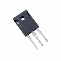
MOSFET N-CH 150V 75A TO-247
Manufacturer
Fairchild Semiconductor
Series
UltraFET™r
Datasheet
1.HUF75852G3.pdf
(10 pages)
Specifications of HUF75852G3
Fet Type
MOSFET N-Channel, Metal Oxide
Fet Feature
Logic Level Gate
Rds On (max) @ Id, Vgs
16 mOhm @ 75A, 10V
Drain To Source Voltage (vdss)
150V
Current - Continuous Drain (id) @ 25° C
75A
Vgs(th) (max) @ Id
4V @ 250µA
Gate Charge (qg) @ Vgs
480nC @ 20V
Input Capacitance (ciss) @ Vds
7690pF @ 25V
Power - Max
500W
Mounting Type
Through Hole
Package / Case
TO-247-3
Configuration
Single
Transistor Polarity
N-Channel
Resistance Drain-source Rds (on)
0.016 Ohms
Drain-source Breakdown Voltage
150 V
Gate-source Breakdown Voltage
+/- 20 V
Continuous Drain Current
75 A
Power Dissipation
500 W
Maximum Operating Temperature
+ 175 C
Mounting Style
Through Hole
Minimum Operating Temperature
- 55 C
Lead Free Status / RoHS Status
Lead free / RoHS Compliant
Available stocks
Company
Part Number
Manufacturer
Quantity
Price
Company:

Part Number:
HUF75852G3
Manufacturer:
FSC
Quantity:
130
Company:
Part Number:
HUF75852G3
Manufacturer:
FAIRCHILD
Quantity:
12 500
Part Number:
HUF75852G3
Manufacturer:
FAIRCHILD/仙童
Quantity:
20 000


Electrical Specifications
Source to Drain Diode Specifications
©2001 Fairchild Semiconductor Corporation
OFF STATE SPECIFICATIONS
Drain to Source Breakdown Voltage
Zero Gate Voltage Drain Current
Gate to Source Leakage Current
ON STATE SPECIFICATIONS
Gate to Source Threshold Voltage
Drain to Source On Resistance
THERMAL SPECIFICATIONS
Thermal Resistance Junction to Case
Thermal Resistance Junction to
Ambient
SWITCHING SPECIFICATIONS (V
Turn-On Time
Turn-On Delay Time
Rise Time
Turn-Off Delay Time
Fall Time
Turn-Off Time
GATE CHARGE SPECIFICATIONS
Total Gate Charge
Gate Charge at 10V
Threshold Gate Charge
Gate to Source Gate Charge
Gate to Drain “Miller” Charge
CAPACITANCE SPECIFICATIONS
Input Capacitance
Output Capacitance
Reverse Transfer Capacitance
Source to Drain Diode Voltage
Reverse Recovery Time
Reverse Recovered Charge
PARAMETER
PARAMETER
T
GS
C
= 25
= 10V)
SYMBOL
SYMBOL
o
V
r
Q
BV
t
Q
DS(ON)
Q
C, Unless Otherwise Specified
t
d(OFF)
C
C
GS(TH)
R
R
I
I
d(ON)
t
g(TOT)
C
Q
Q
GSS
t
Q
V
DSS
OFF
g(TH)
g(10)
OSS
ON
RSS
ISS
t
DSS
t
t
SD
RR
gs
gd
r
rr
JC
f
JA
I
V
V
V
V
I
TO-247
V
V
R
(Figures 18, 19)
V
V
V
V
f = 1MHz
(Figure 12)
I
I
I
I
D
D
SD
SD
SD
SD
DS
DS
GS
GS
DD
GS
GS
GS
GS
GS
DS
= 250 A, V
= 75A, V
= 75A
= 35A
= 75A, dI
= 75A, dI
= 140V, V
= 135V, V
= 25V, V
= 20V
= V
= 75V, I
= 0V to 20V
= 0V to 10V
= 0V to 2V
= 2.0
10V,
DS
, I
GS
D
D
SD
SD
GS
GS
GS
GS
= 10V (Figure 9)
= 75A
TEST CONDITIONS
= 250 A (Figure 10)
TEST CONDITIONS
/dt = 100A/ s
/dt = 100A/ s
= 0V,
= 0V (Figure 11)
= 0V
= 0V, T
V
I
I
(Figures 13, 16, 17)
D
g(REF)
DD
C
= 75A,
= 150
= 75V,
= 1.0mA
o
C
MIN
150
MIN
2
-
-
-
-
-
-
-
-
-
-
-
-
-
-
-
-
-
-
-
-
-
-
-
-
0.013
7690
1650
TYP
151
107
400
215
535
TYP
22
82
15
25
66
-
-
-
-
-
-
-
-
-
-
-
-
-
0.016
MAX
MAX
1830
0.30
17.5
1.25
1.00
250
260
285
480
260
HUF75852G3 Rev. B
260
100
30
1
4
-
-
-
-
-
-
-
-
-
-
UNITS
UNITS
o
o
C/W
C/W
nA
nC
nC
nC
nC
nC
pF
pF
pF
nC
ns
ns
ns
ns
ns
ns
ns
¾
V
V
V
V
A
A
Related parts for HUF75852G3
Image
Part Number
Description
Manufacturer
Datasheet
Request
R

Part Number:
Description:
Fairchild Semiconductor [IGBT MODULE]
Manufacturer:
Fairchild Semiconductor
Datasheet:

Part Number:
Description:
Discrete Semiconductor Modules
Manufacturer:
Fairchild Semiconductor
Part Number:
Description:
Discrete Semiconductor Modules
Manufacturer:
Fairchild Semiconductor
Part Number:
Description:
This N-Channel MOSFET is produced using Fairchild Semiconductor’s advanced Power Trench® process
Manufacturer:
Fairchild Semiconductor
Datasheet:
Part Number:
Description:
This N-Channel MOSFET is produced using Fairchild Semiconductor’s advanced Power Trench® process
Manufacturer:
Fairchild Semiconductor
Datasheet:
Part Number:
Description:
This N-Channel MOSFET is produced using Fairchild Semiconductor’s advanced PowerTrench® process
Manufacturer:
Fairchild Semiconductor
Datasheet:
Part Number:
Description:
This N-Channel MOSFET is produced using Fairchild Semiconductor’s advanced PowerTrench® process
Manufacturer:
Fairchild Semiconductor
Datasheet:
Part Number:
Description:
This N-Channel MOSFET is produced using Fairchild Semiconductor’s advanced Power Trench® process
Manufacturer:
Fairchild Semiconductor
Datasheet:
Part Number:
Description:
This N-Channel logic Level MOSFETs are produced using Fairchild Semiconductor‘s advanced Power Trench® process that has been special tailored to minimize the on-state resistance and yet maintain superior switching performance
Manufacturer:
Fairchild Semiconductor
Datasheet:
Part Number:
Description:
This N-Channel MOSFET is produced using Fairchild Semiconductor’s advanced Power Trench® process
Manufacturer:
Fairchild Semiconductor
Datasheet:
Part Number:
Description:
This N-Channel SyncFET™ is produced using Fairchild Semiconductor’s advanced PowerTrench® process
Manufacturer:
Fairchild Semiconductor
Datasheet:
Part Number:
Description:
This N-Channel SyncFET™ is produced using Fairchild Semiconductor’s advanced PowerTrench® process
Manufacturer:
Fairchild Semiconductor
Datasheet:
Part Number:
Description:
This N-Channel SyncFET™ is produced using Fairchild Semiconductor’s advanced PowerTrench® process
Manufacturer:
Fairchild Semiconductor
Datasheet:
Part Number:
Description:
This N-Channel logic Level MOSFETs are produced using Fairchild Semiconductor‘s advanced Power Trench® process that has been special tailored to minimize the on-state resistance and yet maintain superior switching performance
Manufacturer:
Fairchild Semiconductor
Datasheet:
Part Number:
Description:
This N-Channel MOSFET is produced using Fairchild Semiconductor’s advanced Power Trench® process that has been especially tailored to minimize the on-state resistance and yet maintain superior switching performance
Manufacturer:
Fairchild Semiconductor
Datasheet: