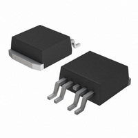
BUK7109-75AIE,118 NXP Semiconductors, BUK7109-75AIE,118 Datasheet - Page 3

BUK7109-75AIE,118
Manufacturer Part Number
BUK7109-75AIE,118
Description
MOSFET N-CH 75V 75A D2PAK
Manufacturer
NXP Semiconductors
Series
TrenchMOS™r
Datasheet
1.BUK7109-75AIE118.pdf
(13 pages)
Specifications of BUK7109-75AIE,118
Package / Case
D²Pak, TO-263 (4 leads + tab)
Fet Type
MOSFET N-Channel, Metal Oxide
Fet Feature
Current Sensing
Rds On (max) @ Id, Vgs
9 mOhm @ 50A, 10V
Drain To Source Voltage (vdss)
75V
Current - Continuous Drain (id) @ 25° C
75A
Vgs(th) (max) @ Id
4V @ 1mA
Gate Charge (qg) @ Vgs
121nC @ 10V
Input Capacitance (ciss) @ Vds
4700pF @ 25V
Power - Max
272W
Mounting Type
Surface Mount
Minimum Operating Temperature
- 55 C
Configuration
Single
Transistor Polarity
N-Channel
Resistance Drain-source Rds (on)
0.009 Ohm @ 10 V
Drain-source Breakdown Voltage
75 V
Gate-source Breakdown Voltage
20 V
Continuous Drain Current
120 A
Power Dissipation
272000 mW
Maximum Operating Temperature
+ 175 C
Mounting Style
SMD/SMT
Lead Free Status / RoHS Status
Lead free / RoHS Compliant
Lead Free Status / RoHS Status
Lead free / RoHS Compliant, Lead free / RoHS Compliant
Other names
934057281118
BUK7109-75AIE /T3
BUK7109-75AIE /T3
BUK7109-75AIE /T3
BUK7109-75AIE /T3
NXP Semiconductors
4. Limiting values
Table 4.
In accordance with the Absolute Maximum Rating System (IEC 60134).
BUK7109-75AIE_2
Product data sheet
Symbol
V
V
V
I
I
P
I
T
T
Source-drain diode
I
I
Avalanche ruggedness
E
Electrostatic discharge
V
D
DM
GS(CL)
S
SM
stg
j
DS
DGS
GS
tot
DS(AL)S
esd
Limiting values
Parameter
drain-source voltage
drain-gate voltage
gate-source voltage
drain current
peak drain current
total power dissipation
gate-source clamping
current
storage temperature
junction temperature
source current
peak source current
non-repetitive
drain-source avalanche
energy
electrostatic discharge
voltage
[1]
[2]
Current is limited by power dissipation chip rating.
Continuous current is limited by package.
Conditions
T
T
see
T
T
T
continuous
pulsed; t
T
t
I
T
HBM; C = 100 pF; R = 1.5 kΩ
p
D
j
mb
mb
mb
mb
mb
j(init)
≤ 10 µs; pulsed; T
≥ 25 °C; T
= 75 A; V
= 25 °C; V
Figure 3
= 100 °C; V
= 25 °C; t
= 25 °C; see
= 25 °C
= 25 °C; unclamped
p
= 5 ms; δ 0.01
Rev. 02 — 10 February 2009
sup
j
≤ 175 °C
p
GS
≤ 75 V; R
≤ 10 µs; pulsed; see
GS
Figure 1
= 10 V; see
= 10 V; see
mb
= 25 °C
GS
= 50 Ω; V
Figure
Figure 2
N-channel TrenchPLUS standard level FET
Figure 3
2;
GS
= 10 V;
BUK7109-75AIE
[1]
[2]
[2]
[1]
[2]
Min
-
-
-20
-
-
-
-
-
-
-
-55
-55
-
-
-
-
-
© NXP B.V. 2009. All rights reserved.
Max
75
75
20
120
75
75
480
272
10
50
175
175
120
75
480
739
6
Unit
V
V
V
A
A
A
A
W
mA
mA
°C
°C
A
A
A
mJ
kV
3 of 13


