BSP299 L6327 Infineon Technologies, BSP299 L6327 Datasheet
BSP299 L6327
Specifications of BSP299 L6327
SP000089200


Related parts for BSP299 L6327


BSP299 L6327 Summary of contents
Page 1
SIPMOS Small-Signal Transistor • N channel • Enhancement mode • Avalanche rated • 2.1 ... 4.0 V GS(th) • Pb-free lead plating; RoHS compliant V Type DS BSP 299 500 V Type Pb-free BSP 299 Yes Maximum ...
Page 2
Maximum Ratings Parameter Chip or operating temperature Storage temperature Thermal resistance, chip to ambient air Therminal resistance, junction-soldering point DIN humidity category, DIN 40 040 IEC climatic category, DIN IEC 68-1 1) Transistor on epoxy pcb ...
Page 3
Electrical Characteristics Parameter Dynamic Characteristics Transconductance ≥ 0 DS(on)max, D Input capacitance = MHz ...
Page 4
Electrical Characteristics Parameter Reverse Diode Inverse diode continuous forward current = 25 ° Inverse diode direct current,pulsed °C A Inverse diode forward voltage = 0 ...
Page 5
Power dissipation = ƒ tot A 2.0 W 1.6 P tot 1.4 1.2 1.0 0.8 0.6 0.4 0.2 0 Safe operating area I =f parameter : ...
Page 6
Typ. output characteristics = ƒ parameter ° 0.9 0.9 0 tot d 10V l c ...
Page 7
Drain-source on-resistance = ƒ (on) j parameter 0 Ω ( typ ...
Page 8
Avalanche energy E AS parameter 1 Ω 163 140 mJ 120 E 110 AS 100 ...
Page 9
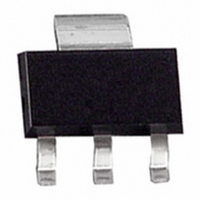
Package outlines SOT-223 Dimensions in mm Rev 2.1 9 BSP 299 2009-03-25 ...
Page 10
... Infineon Technologies Office. Infineon Technologies components may be used in life-support devices or systems only with the express written approval of Infineon Technologies failure of such components can reasonably be expected to cause the failure of that life-support device or system or to affect the safety or effectiveness of that device or system ...