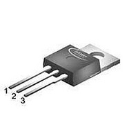
IPP77N06S2-12 Infineon Technologies, IPP77N06S2-12 Datasheet
IPP77N06S2-12
Specifications of IPP77N06S2-12
Available stocks


Related parts for IPP77N06S2-12

IPP77N06S2-12 Summary of contents
Page 1
... Rev. 1.0 Product Summary PG-TO263-3-2 Ordering Code SP0002-18173 SP0002-18172 Symbol Conditions I T =25 ° =100 ° = =25 °C D,pulse =25 °C tot stg page 1 IPB77N06S2-12 IPP77N06S2-12 DS (SMD version) DS(on),max D PG-TO220-3-1 Marking 2N0612 2N0612 Value = 308 280 ±20 158 -55 ... +175 55/175/ 11 Unit °C 2005-12-27 ...
Page 2
... (BR)DSS =93 µA GS(th = DSS T =25 ° = =125 ° = GSS = =38 A, DS( SMD version page 2 IPB77N06S2-12 IPP77N06S2-12 Values min. typ. max 0. 2.1 3 100 = 100 - 9.8 12.0 - 9.5 11.7 Unit K µA nA mΩ 2005-12-27 ...
Page 3
... d(off = = plateau =25 ° S,pulse = =25 ° = /dt =100 A/µ 0.95 K/W the chip is able to carry 25°C. For detailed thJC 2 (one layer, 70 µm thick) copper area for drain page 3 IPB77N06S2-12 IPP77N06S2-12 Values min. typ. max. - 1770 = 460 - 120 - = 5 0 Unit - 308 1 2005-12-27 ...
Page 4
... DS C parameter 1000 100 Rev. 1.0 2 Drain current 100 150 200 4 Max. transient thermal impedance Z = f(t thJC parameter µs 10 µ 100 µ 100 [V] page 4 IPB77N06S2-12 IPP77N06S2- ≥ 100 150 T [° 0.5 0.1 0.05 0.01 single pulse - [s] p 200 - 2005-12-27 ...
Page 5
... Typ. transfer characteristics parameter 120 100 175 ° Rev. 1.0 6 Typ. drain-source on-state resistance DS(on) parameter 5 4 [V] 8 Typ. Forward transconductance parameter: g 150 125 100 °C -55 ° [V] page 5 IPB77N06S2-12 IPP77N06S2- ° 5 [ 25° 100 150 I [ 100 120 200 2005-12-27 ...
Page 6
... Typ. gate threshold voltage V = f(T GS(th) parameter 3.5 3 2.5 2 1.5 1 100 140 180 12 Typical forward diode characteristicis IF = f(V SD parameter Ciss Coss 1 10 Crss [V] page 6 IPB77N06S2-12 IPP77N06S2- 465 µA 93 µA -60 - 100 T [° °C 175 °C 0 0.2 0.4 0.6 0 [V] SD 140 180 1.2 1.4 2005-12-27 ...
Page 7
... A 500 50 A 400 300 77 A 200 100 100 T [° Typ. drain-source breakdown voltage BR(DSS -60 - [°C] j Rev. 1.0 14 Typ. gate charge V = f(Q GS gate 150 200 0 16 Gate charge waveforms 100 140 180 page 7 IPB77N06S2-12 IPP77N06S2- pulsed [nC] gate gate gate 2005-12-27 60 ...
Page 8
... Life support devices or systems are intended to be implanted in the human body support and/or maintain and sustain and/or protect human life. If they fail reasonable to assume that the health of the user or other persons may be endangered. Rev. 1.0 page 8 IPB77N06S2-12 IPP77N06S2-12 2005-12-27 ...