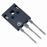
SPW52N50C3 Infineon Technologies, SPW52N50C3 Datasheet - Page 2

SPW52N50C3
Manufacturer Part Number
SPW52N50C3
Description
MOSFET N-CH 560V 52A TO-247
Manufacturer
Infineon Technologies
Series
CoolMOS™r
Specifications of SPW52N50C3
Package / Case
TO-247-3 (Straight Leads)
Fet Type
MOSFET N-Channel, Metal Oxide
Fet Feature
Standard
Rds On (max) @ Id, Vgs
70 mOhm @ 30A, 10V
Drain To Source Voltage (vdss)
560V
Current - Continuous Drain (id) @ 25° C
52A
Vgs(th) (max) @ Id
3.9V @ 2.7mA
Gate Charge (qg) @ Vgs
290nC @ 10V
Input Capacitance (ciss) @ Vds
6800pF @ 25V
Power - Max
417W
Mounting Type
Through Hole
Minimum Operating Temperature
- 55 C
Configuration
Single
Transistor Polarity
N-Channel
Resistance Drain-source Rds (on)
0.07 Ohm @ 10 V
Drain-source Breakdown Voltage
560 V
Gate-source Breakdown Voltage
+/- 20 V
Continuous Drain Current
52 A
Power Dissipation
417000 mW
Maximum Operating Temperature
+ 150 C
Mounting Style
Through Hole
Continuous Drain Current Id
52A
Drain Source Voltage Vds
560V
On Resistance Rds(on)
70mohm
Rds(on) Test Voltage Vgs
10V
Threshold Voltage Vgs Typ
3V
Rohs Compliant
Yes
Lead Free Status / RoHS Status
Lead free / RoHS Compliant
Lead Free Status / RoHS Status
Lead free / RoHS Compliant, Lead free / RoHS Compliant
Other names
SP000014626
SPW52N50C3
SPW52N50C3IN
SPW52N50C3X
SPW52N50C3XK
SPW52N50C3
SPW52N50C3IN
SPW52N50C3X
SPW52N50C3XK
Available stocks
Company
Part Number
Manufacturer
Quantity
Price
Company:
Part Number:
SPW52N50C3
Manufacturer:
INFINEON
Quantity:
149
Part Number:
SPW52N50C3
Manufacturer:
INFINEON/英飞凌
Quantity:
20 000
Please note the new package dimensions arccording to PCN 2009-134-A
Maximum Ratings
Parameter
Drain Source voltage slope
V
Thermal Characteristics
Parameter
Thermal resistance, junction - case
Thermal resistance, junction - ambient, leaded
Soldering temperature, wavesoldering
1.6 mm (0.063 in.) from case for 10s
Electrical Characteristics, at Tj=25°C unless otherwise specified
Parameter
Drain-source breakdown voltage V
Drain-Source avalanche
breakdown voltage
Gate threshold voltage
Zero gate voltage drain current
Gate-source leakage current
Drain-source on-state resistance R
Gate input resistance
Rev. 2.6
DS
= 400 V, I
D
= 52 A, T
j
= 125 °C
V
V
I
I
R
Symbol
DSS
GSS
(BR)DSS V
(BR)DS
GS(th)
DS(on)
G
Page 2
V
I
V
T
T
V
V
T
T
f=1MHz, open Drain
D
j
j
j
j
GS
GS
DS
GS
GS
=25°C,
=150°C
=25°C
=150°C
=2700μΑ, V
Conditions
=500V, V
=0V, I
=0V, I
=20V, V
=10V, I
Symbol
d v /d t
Symbol
R
R
T
D
D
sold
=0.25mA
=20A
thJC
thJA
D
DS
GS
=30A,
GS
=0V
=0V,
=V
DS
min.
min.
500
2.1
-
-
-
-
-
-
-
-
-
-
Values
Values
Value
0.06
0.16
typ.
typ.
600
0.5
0.7
50
3
SPW52N50C3
-
-
-
-
-
-
2008-02-11
max.
max.
0.07
260
250
100
0.3
3.9
62
25
-
-
-
-
Unit
V/ns
Unit
K/W
°C
Unit
V
μA
nA
Ω


