RFD15P05 Fairchild Semiconductor, RFD15P05 Datasheet - Page 2
RFD15P05
Manufacturer Part Number
RFD15P05
Description
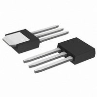
MOSFET P-CH 50V 15A I-PAK
Manufacturer
Fairchild Semiconductor
Datasheet
1.RFD15P05.pdf
(8 pages)
Specifications of RFD15P05
Fet Type
MOSFET P-Channel, Metal Oxide
Fet Feature
Standard
Rds On (max) @ Id, Vgs
150 mOhm @ 15A, 10V
Drain To Source Voltage (vdss)
50V
Current - Continuous Drain (id) @ 25° C
15A
Vgs(th) (max) @ Id
4V @ 250µA
Gate Charge (qg) @ Vgs
150nC @ 20V
Input Capacitance (ciss) @ Vds
1150pF @ 25V
Power - Max
80W
Mounting Type
Through Hole
Package / Case
IPak, TO-251, DPak, VPak (3 straight leads + tab)
Lead Free Status / RoHS Status
Contains lead / RoHS non-compliant
Available stocks
Company
Part Number
Manufacturer
Quantity
Price
Company:

Part Number:
RFD15P05
Manufacturer:
HARRIS
Quantity:
10 000
Company:
Part Number:
RFD15P05SM
Manufacturer:
INTERSIL
Quantity:
1 062


©2002 Fairchild Semiconductor Corporation
Absolute Maximum Ratings
Drain Source Voltage (Note 1) . . . . . . . . . . . . . . . . . . . . . . . . . . . . . . . . . . . . . . . . . . . . . . V
Drain Gate Voltage (R
Gate Source Voltage . . . . . . . . . . . . . . . . . . . . . . . . . . . . . . . . . . . . . . . . . . . . . . . . . . . . . . V
Drain Current Continuous . . . . . . . . . . . . . . . . . . . . . . . . . . . . . . . . . . . . . . . . . . . . . . . . . . . . I
Single Pulse Avalanche Rating . . . . . . . . . . . . . . . . . . . . . . . . . . . . . . . . . . . . . . . . . . . . . . E
Power Dissipation . . . . . . . . . . . . . . . . . . . . . . . . . . . . . . . . . . . . . . . . . . . . . . . . . . . . . . . . . P
Operating and Storage Temperature . . . . . . . . . . . . . . . . . . . . . . . . . . . . . . . . . . . . . . T
Maximum Temperature for Soldering
CAUTION: Stresses above those listed in “Absolute Maximum Ratings” may cause permanent damage to the device. This is a stress only rating and operation of the
device at these or any other conditions above those indicated in the operational sections of this specification is not implied.
NOTE:
Electrical Specifications
Source to Drain Diode Specifications
NOTES:
Drain to Source Breakdown Voltage
Gate Threshold Voltage
Zero Gate Voltage Drain Current
Gate to Source Leakage Current
Drain to Source On Resistance
Turn-On Time
Turn-On Delay Time
Rise Time
Turn-Off Delay Time
Fall Time
Turn-Off Time
Total Gate Charge
Gate Charge at -10V
Threshold Gate Charge
Input Capacitance
Output Capacitance
Reverse Transfer Capacitance
Thermal Resistance Junction to Case
Thermal Resistance Junction to Ambient
Source to Drain Diode Voltage
Reverse Recovery Time
1. T
2. Pulse test: pulse duration ≤ 300ms, duty cycle ≤ 2%.
3. Repetitive rating: pulse width limited by maximum junction temperature. See Transient Thermal Impedance curve (Figure 3).
Pulsed (Note 3) . . . . . . . . . . . . . . . . . . . . . . . . . . . . . . . . . . . . . . . . . . . . . . . . . . . . . . . . . I
Derate above 25
Leads at 0.063in (1.6mm) from Case for 10s. . . . . . . . . . . . . . . . . . . . . . . . . . . . . . . . . . . . T
Package Body for 10s, See Techbrief 334 . . . . . . . . . . . . . . . . . . . . . . . . . . . . . . . . . . . . T
J
= 25
o
C to 150
PARAMETER
PARAMETER
o
C. . . . . . . . . . . . . . . . . . . . . . . . . . . . . . . . . . . . . . . . . . . . . . . . . . . . . . . . . .
o
G
C.
= 20K Ω ) (Note 1) . . . . . . . . . . . . . . . . . . . . . . . . . . . . . . . . . . . . . V
T
C
T
= 25
C
= 25
o
C, Unless Otherwise Specified
o
SYMBOL
SYMBOL
C, Unless Otherwise Specified
V
Q
r
t
Q
BV
Q
t
DS(ON)
D(OFF)
C
C
GS(TH)
D(ON)
R
I
G(TOT)
C
R
I
t
V
G(-10)
GSS
t
G(TH)
t
DSS
OFF
OSS
ON
RSS
RR
t
t
ISS
θ JC
θ JA
SD
DSS
R
F
I
I
I
V
V
V
V
I
V
R
V
V
V
V
f = 1MHz (Figure 12)
TO-220AB, TO-251AA, TO-252AA
TO-251AA, TO-252AA
TO-220AB
SD
SD
D
D
GS
DS
DS
GS
DD
GS
GS
GS
DS
L
= 250 µ A, V
= 15A, V
= 3.3 Ω , V
= -15A
= -15A, dI
= Rated BV
= 0.8 x Rated BV
= -25V, V
= V
= ± 20V
= -25V, I
= 0V to -20V V
= 0V to -10V
= 0V to -2V
DS
, I
GS
TEST CONDITIONS
TEST CONDITIONS
GS
D
SD
D
GS
GS
= -10V (Figure 9)
= 250 µ A
≈
/dt = -100A/ µ s
DSS
= -10V
= 0V (Figure 11)
7.5A, R
= 0V
R
I
G(REF)
DD
L
DSS,
= 2.67 Ω,
= -40V, I
G
J
T
= 12.5 Ω ,
, T
= -0.65mA
C
DGR
DSS
STG
= 150
DM
pkg
GS
AS
D
D
L
D
= 15A,
o
C
Refer to Peak Current Curve
RFD15P05, RFD15P05SM,
Refer to UIS Curve
RFP15P05
-55 to 175
0.533
MIN
-2.0
-50
MIN
± 20
300
260
-50
-50
-15
RFD15P05, RFD15P05SM, RFP15P05 Rev. B
80
-
-
-
-
-
-
-
-
-
-
-
-
-
-
-
-
-
-
-
-
-
1150
TYP
300
TYP
16
30
50
20
56
-
-
-
-
-
-
-
-
-
-
-
-
-
-
-
-
0.150
1.875
MAX
± 100
MAX
62.5
-4.0
100
150
100
-1.5
125
3.5
25
60
75
-1
-
-
-
-
-
-
-
-
UNITS
W/
o
o
o
UNITS
UNITS
W
V
V
V
A
o
o
o
C
C
C
o
C/W
C/W
C/W
µ A
µ A
nA
nC
nC
nC
pF
pF
pF
ns
ns
ns
ns
ns
ns
ns
C
Ω
V
V
V
Related parts for RFD15P05
Image
Part Number
Description
Manufacturer
Datasheet
Request
R

Part Number:
Description:
Fairchild Semiconductor [IGBT MODULE]
Manufacturer:
Fairchild Semiconductor
Datasheet:

Part Number:
Description:
Discrete Semiconductor Modules
Manufacturer:
Fairchild Semiconductor
Part Number:
Description:
Discrete Semiconductor Modules
Manufacturer:
Fairchild Semiconductor
Part Number:
Description:
This N-Channel MOSFET is produced using Fairchild Semiconductor’s advanced Power Trench® process
Manufacturer:
Fairchild Semiconductor
Datasheet:
Part Number:
Description:
This N-Channel MOSFET is produced using Fairchild Semiconductor’s advanced Power Trench® process
Manufacturer:
Fairchild Semiconductor
Datasheet:
Part Number:
Description:
This N-Channel MOSFET is produced using Fairchild Semiconductor’s advanced PowerTrench® process
Manufacturer:
Fairchild Semiconductor
Datasheet:
Part Number:
Description:
This N-Channel MOSFET is produced using Fairchild Semiconductor’s advanced PowerTrench® process
Manufacturer:
Fairchild Semiconductor
Datasheet:
Part Number:
Description:
This N-Channel MOSFET is produced using Fairchild Semiconductor’s advanced Power Trench® process
Manufacturer:
Fairchild Semiconductor
Datasheet:
Part Number:
Description:
This N-Channel logic Level MOSFETs are produced using Fairchild Semiconductor‘s advanced Power Trench® process that has been special tailored to minimize the on-state resistance and yet maintain superior switching performance
Manufacturer:
Fairchild Semiconductor
Datasheet:
Part Number:
Description:
This N-Channel MOSFET is produced using Fairchild Semiconductor’s advanced Power Trench® process
Manufacturer:
Fairchild Semiconductor
Datasheet:
Part Number:
Description:
This N-Channel SyncFET™ is produced using Fairchild Semiconductor’s advanced PowerTrench® process
Manufacturer:
Fairchild Semiconductor
Datasheet:
Part Number:
Description:
This N-Channel SyncFET™ is produced using Fairchild Semiconductor’s advanced PowerTrench® process
Manufacturer:
Fairchild Semiconductor
Datasheet:
Part Number:
Description:
This N-Channel SyncFET™ is produced using Fairchild Semiconductor’s advanced PowerTrench® process
Manufacturer:
Fairchild Semiconductor
Datasheet:
Part Number:
Description:
This N-Channel logic Level MOSFETs are produced using Fairchild Semiconductor‘s advanced Power Trench® process that has been special tailored to minimize the on-state resistance and yet maintain superior switching performance
Manufacturer:
Fairchild Semiconductor
Datasheet:
Part Number:
Description:
This N-Channel MOSFET is produced using Fairchild Semiconductor’s advanced Power Trench® process that has been especially tailored to minimize the on-state resistance and yet maintain superior switching performance
Manufacturer:
Fairchild Semiconductor
Datasheet: