FDP4020P Fairchild Semiconductor, FDP4020P Datasheet
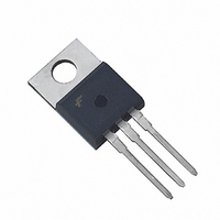
MOSFET P-CH 20V 16A TO-220AB

FDP4020P

Manufacturer Part Number
FDP4020P
Description
MOSFET P-CH 20V 16A TO-220AB
Manufacturer
Fairchild Semiconductor
Datasheet

Specifications of FDP4020P

Fet Type
MOSFET P-Channel, Metal Oxide
Fet Feature
Logic Level Gate
Rds On (max) @ Id, Vgs
80 mOhm @ 8A, 4.5V
Drain To Source Voltage (vdss)
20V
Current - Continuous Drain (id) @ 25° C
16A
Vgs(th) (max) @ Id
1V @ 250µA
Gate Charge (qg) @ Vgs
13nC @ 4.5V
Input Capacitance (ciss) @ Vds
665pF @ 10V
Power - Max
37.5W
Mounting Type
Through Hole
Package / Case
TO-220-3 (Straight Leads)
Lead Free Status / RoHS Status
Lead free / RoHS Compliant

Available stocks

Company
Part Number
Manufacturer
Quantity
Price
Part Number:
FDP4020P
Manufacturer:
FAIRCHILD
Quantity:
12 500
Part Number:
FDP4020P
Manufacturer:
FAIRCHILD/仙童
Quantity:
20 000
2000 Fairchild Semiconductor International
FDP4020P/FDB4020P
P-Channel 2.5V Specified Enhancement Mode Field Effect Transistor
General Description
This P-Channel low threshold MOSFET has been
designed for use as a linear pass element for low voltage
outputs. In addition, the part may be used as a low voltage
load switch when switching outputs on or off for power
management.The part may also be used in conjunction
with DC-DC converters requiring P-Channel.
A bsolute M axim um Ratings
V
V
I
P
T
Therm al C haracteristics
R
R
Package O utlines and O rdering Inform ation
Sym bol
D
J
DSS
G SS
D
, T
JC
JA
D evice M arking
STG
FDP 4020P
Drain-S ource V oltage
G ate-S ource V oltage
Drain Current
Total P ower Dissipation @ T
O perating and S torage Junction Tem perature Range
Therm al Resistance, Junction-to- Case
Therm al Resistance, Junction-to- A m bient
- Continuous
- P ulsed
Derate above 25 C
Param eter
FDP 4020P
D evice
C
= 25 C
T
A
= 25°C unless otherw ise noted
R eel Size
Features
• -16 A, -20 V. R
• Critical DC electrical parameters specified at elevated
• High density cell design for extremely low R
• TO-220 and TO-263 (D 2 PAK) package for both
• 175 C maximum junction temperature rating.
13’’
through hole and surface mount applications.
temperature.
(N ote 1)
FD P4020P
R
DS(on)
DS(on)
62.5
Tape W idth
= 0.08
12m m
= 0.11
-65 to +175
37.5
0.25
-20
-16
-48
4
8
FD B 4020P
@ V
@ V
G
GS
GS
40
= -4.5 V
= -2.5 V.
September 2000
2500 units
Q uantity
DS(on)
D
S
.
U nits
FDP4020P Rev. B
W / C
C/W
C/W
W
V
V
A
C

Related parts for FDP4020P

FDP4020P Summary of contents

Page 1

... A FD P4020P = ote 1) D evice R eel Size FDP 4020P 13’’ September 2000 = 0. -4.5 V DS(on 0. -2.5 V. DS(on) GS DS(on 4020P U nits - -16 A -48 37 -65 to +175 C C/W 4 62.5 40 C/W Tape W idth Q uantity 12m m 2500 units FDP4020P Rev. B ...

Page 2

... A, Referenced -4.5 V -4.5 V A,T =125 -2 1.0 MHz -4 GEN - -4 (Note 2) (Note -16 A (Note 2.0% Min Typ Max Units -20 V -28 mV 100 nA -100 nA -0.4 -0. mV/ C 0.068 0.08 0.098 0.13 0.096 0.110 - 665 pF 270 9 1.3 nC 2.2 nC -16 A -48 -1 pad FDP4020P Rev. B ...

Page 3

... C 1 0.01 0.0001 0 3 3.5 4 Figure 6. Body Diode Forward Voltage Variation with Source Current -2.5V -3.0V -3.5V -4.0V -4. DIRAIN CURRENT ( - 125 2.5 3 3 GATE TO SOURCE VOLTAGE ( 125 -55 C 0.4 0.8 1 BODY DIODE FORWARD VOLTAGE (V) SD and Temperature. FDP4020P Rev 1.6 ...

Page 4

... Thermal characterization performed using the conditions described in Note 1. Transient themal response will change depending on the circuit board design MHz ISS C OSS C RSS DRAIN TO SOURCE VOLTAGE (V) DS SINGLE PULSE C 0.001 0.01 0 SINGLE PULSE TIME (SEC) Power Dissipation. R ( 4°C/W JC P(pk ( Duty Cycle FDP4020P Rev ...

Page 5

TRADEMARKS DISCLAIMER LIFE SUPPORT POLICY PRODUCT STATUS DEFINITIONS Definition of Terms Datasheet Identification Product Status Definition ...

Related keywords