FQPF6N90 Fairchild Semiconductor, FQPF6N90 Datasheet
FQPF6N90
Specifications of FQPF6N90
Available stocks


Related parts for FQPF6N90


FQPF6N90 Summary of contents
Page 1
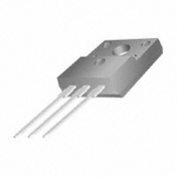
... Purposes, 1/8” from case for 5-seconds THERMAL RESISTANCE Symbol Characteristics R Junction-to-Case JC R Junction-to-Ambient JA 1999 Fairchild Semiconductor Corporation Value 900 = 100 C) 2.1 C 13.6 710 3.4 5 +150 300 Typ. FQPF6N90 BV = 900V DSS R = 1.9 DS(ON 3.4A D TO-220F Gate 2. Drain 3. Source Units V/ Max. Units 2.25 C/W 62 ...
Page 2
... FQPF6N90 ELECTRICAL CHARACTERISTICS Symbol Characteristics BV Drain-Source Breakdown Voltage DSS BV/ T Breakdown Voltage Temp. Coeff Gate Threshold Voltage GS(th) Gate-Source Leakage, Forward I GSS Gate-Source Leakage, Reverse I Drain-to-Source Leakage Current DSS Static Drain-Source R DS(on) On-State Resistance g Forward Transconductance fs C Input Capacitance iss C Output Capacitance ...
Page 3
QFET N-CHANNEL Fig 1. Output Characteristics V GS Top : 15 10.0 V 8.0 V 7.0 V 6.5 V 6.0 V 5.5 V Bottom : 5 ¡Ø Note : 1. 250¥ìs Pulse ...
Page 4
... FQPF6N90 Fig 7. Breakdown Voltage vs. Temperature 1.2 1.1 1.0 0.9 0.8 -100 - Junction Temperature [ J Fig 9. Max. Safe Operating Area 2 10 Operation in This Area is Limited by R DS(on ¡Ø Notes : 150 Single Pulse - Drain-Source Voltage [ 3.0 2.5 2.0 1.5 1.0 ¡Ø Note : 1 ...
Page 5
... Fig 14. Unclamped Inductive Switching Test Circuit & Waveforms 10V Fig 12. Gate Charge Test Circuit & Waveform V GS Same Type as DUT 10V V DS DUT 0.5 rated DUT DSS DSS DUT DD DD FQPF6N90 Charge 90% 90% 10% 10 d(on) d(on d(off) d(off off off BV BV DSS DSS ---- ---- ---- ---- ...
Page 6
... FQPF6N90 Fig 15. Peak Diode Recovery dv/dt Test Circuit & Waveforms Driver ) ( Driver ) DUT ) ( DUT ) DUT ) ( DUT ) 6 DUT + Driver R G Same Type as DUT • dv/dt controlled by R • I controlled by pulse period S Gate Pulse Width Gate Pulse Width Gate Pulse Width -------------------------- -------------------------- ...
Page 7
... QFET N-CHANNEL TO-220F Package Dimensions TO-220F (FS PKG CODE AQ) 10.16 (7.00) MAX1.47 0.80 0.10 #1 0.35 0.10 2.54TYP [2.54 ] 0.20 9.40 ø3.18 0.20 0.10 (1.00x45 ) 0.50 2.54TYP [2.54 ] 0.20 0.20 FQPF6N90 2.54 0.20 (0.70) +0.10 2.76 –0.05 0.20 Dimensions in Millimeters September 1999, Rev B 7 ...
Page 8
... TRADEMARKS The following are registered and unregistered trademarks Fairchild Semiconductor owns or is authorized to use and is not intended exhaustive list of all such trademarks. ACEx™ CoolFET™ CROSSVOLT™ CMOS FACT™ FACT Quiet Series™ ® FAST FASTr™ GTO™ ...