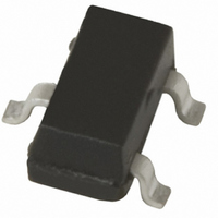
BSS83PE6327 Infineon Technologies, BSS83PE6327 Datasheet - Page 2

BSS83PE6327
Manufacturer Part Number
BSS83PE6327
Description
MOSFET P-CH 60V 330MA SOT-23
Manufacturer
Infineon Technologies
Series
SIPMOS®r
Datasheet
1.BSS83PE6327.pdf
(9 pages)
Specifications of BSS83PE6327
Fet Type
MOSFET P-Channel, Metal Oxide
Fet Feature
Logic Level Gate
Rds On (max) @ Id, Vgs
2 Ohm @ 330mA, 10V
Drain To Source Voltage (vdss)
60V
Current - Continuous Drain (id) @ 25° C
330mA
Vgs(th) (max) @ Id
2V @ 80µA
Gate Charge (qg) @ Vgs
3.57nC @ 10V
Input Capacitance (ciss) @ Vds
78pF @ 25V
Power - Max
360mW
Mounting Type
Surface Mount
Package / Case
SOT-23-3, TO-236-3, Micro3™, SSD3, SST3
Lead Free Status / RoHS Status
Lead free / RoHS Compliant
Other names
BSS83PE6327INTR
BSS83PE6327XT
BSS83PE6327XTINTR
BSS83PE6327XTINTR
SP000012075
BSS83PE6327XT
BSS83PE6327XTINTR
BSS83PE6327XTINTR
SP000012075
Electrical Characteristics, at T
Parameter
Static Characteristics
Drain- source breakdown voltage
V
Gate threshold voltage, V
I
Zero gate voltage drain current
V
V
Gate-source leakage current
V
Drain-Source on-state resistance
V
Drain-Source on-state resistance
V
1 Device on 40mm*40mm*1.5mm epoxy PCB FR4 with 6cm 2 (one layer, 70 µm thick) copper area for drain
connection. PCB is vertical without blown air.
Thermal Characteristics
Parameter
Characteristics
Thermal resistance, junction - soldering point
( Pin 3 )
SMD version, device on PCB:
@ min. footprint
@ 6 cm
D
GS
DS
DS
GS
GS
GS
= -80 µA
= -60 V, V
= -60 V, V
= 0 V, I
= -20 V, V
= -4.5 V, I
= -10 V, I
2
cooling area
D
= -250 µA
D
D
GS
GS
DS
= -0.33 A
= -0.27 A
= 0 V, T
= 0 V, T
= 0 V
1)
GS
j
j
= 25 °C
= 125 °C
= V
j
DS
= 25 °C, unless otherwise specified
Preliminary data
Page 2
Symbol
V
V
I
I
R
R
Symbol
R
R
DSS
GSS
(BR)DSS
GS(th)
DS(on)
DS(on)
thJS
thJA
min.
min.
-60
-1
-
-
-
-
-
-
-
-
Values
Values
typ.
-1.5
-0.1
typ.
-10
-10
1.4
2
-
-
-
-
max.
max.
-100
-100
150
350
300
-2
-1
1999-09-16
3
2
-
BSS 83 P
Unit
V
µA
nA
Unit
K/W
K/W


