2N5555 Fairchild Semiconductor, 2N5555 Datasheet
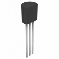
AMP N-CHAN JFET 25V TO-92

2N5555

Manufacturer Part Number
2N5555
Description
AMP N-CHAN JFET 25V TO-92
Manufacturer
Fairchild Semiconductor
Datasheets

Specifications of 2N5555

Transistor Type
N-Channel JFET
Voltage - Rated
25V
Current Rating
15mA
Package / Case
TO-92
Configuration
Single
Transistor Polarity
N-Channel
Power Dissipation
350 mW
Gate-source Breakdown Voltage
- 25 V
Drain Current (idss At Vgs=0)
1 mA to 8 mA
Resistance Drain-source Rds (on)
150 Ohms
Maximum Operating Temperature
+ 150 C
Maximum Drain Gate Voltage
25 V
Minimum Operating Temperature
- 55 C
Mounting Style
Through Hole
Lead Free Status / RoHS Status
Lead free / RoHS Compliant
Power - Output
-
Frequency
-
Gain
-
Noise Figure
-
Current - Test
-
Voltage - Test
-
Lead Free Status / Rohs Status
Lead free / RoHS Compliant

Available stocks

Company
Part Number
Manufacturer
Quantity
Price
Part Number:
2N5555
Manufacturer:
FSC
Quantity:
420
Part Number:
2N5555
Manufacturer:
FAIRCHILD
Quantity:
38 000
Part Number:
2N5555
Manufacturer:
VISHAY
Quantity:
3 000
Part Number:
2N5555
Manufacturer:
ST/MOTO
Quantity:
20 000
2N5555 Rev. 1.0.0
© 2007 Fairchild Semiconductor Corporation
2N5555
N-Channel RF Amplifier
• This device is designed primarily for electronic switching applications such as low on resistance analog switching.
• Sourced from process 50.
Absolute Maximum Ratings*
* This ratings are limiting values above which the serviceability of any semiconductor device may be impaired.
NOTES:
1) These rating are based on a maximum junction temperature of 150 degrees C.
2) These are steady limits. The factory should be consulted on applications involving pulsed or low duty cycle operations.
Thermal Characteristics
V
V
I
T
P
R
R
GF
DG
GS
J
D
qJC
qJA
, T
Symbol
Symbol
STG
Drain-Gate Voltage
Gate-Source Voltage
Forward Gate Current
Operating and Storage Junction Temperature Range
Total Device Dissipation
Derate above 25°C
Thermal Resistance, Junction to Case
Thermal Resistance, Junction to Ambient
T
a
=25°C unless otherwise noted
T
Parameter
Parameter
a
=25°C unless otherwise noted
1. Gate 2. Source 3. Drain
1
1
TO-92
-55 ~ 150
Value
Max.
350
125
357
-25
2.8
25
10
www.fairchildsemi.com
May 2008
Units
Units
mW/°C
°C/W
°C/W
mW
mA
°C
V
V

Related parts for 2N5555

2N5555 Summary of contents

Page 1

... Symbol Total Device Dissipation P D Derate above 25°C R Thermal Resistance, Junction to Case qJC R Thermal Resistance, Junction to Ambient qJA © 2007 Fairchild Semiconductor Corporation 2N5555 Rev. 1.0.0 TO- Gate 2. Source 3. Drain T =25°C unless otherwise noted a Parameter T =25°C unless otherwise noted a Parameter ...

Page 2

... Zero-Gate Voltage Drain Current * DSS R (on) Drain-Source On Resistance DS Small Signal Characteristics C Input Capacitance iss C Reverse Transfer Capacitance rss * Pulse Test: Pulse Width £ 300ms, Duty Cycle = 2% © 2007 Fairchild Semiconductor Corporation 2N5555 Rev. 1.0.0 T =25°C unless otherwise noted a Test Condition I = 10mA 15V 25° ...

Page 3

... Advance Information Formative or In Design Preliminary First Production No Identification Needed Full Production Obsolete Not In Production © 2007 Fairchild Semiconductor Corporation 2N5555 Rev. 1.0.0 Green FPS™ Power247 Green FPS™ e-Series™ POWEREDGE GTO™ Power-SPM™ i-Lo™ PowerTrench IntelliMAX™ ...

Related keywords