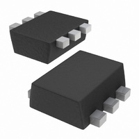
BF1208,115 NXP Semiconductors, BF1208,115 Datasheet - Page 15

BF1208,115
Manufacturer Part Number
BF1208,115
Description
MOSFET N-CH DUAL GATE SSMINI-6
Manufacturer
NXP Semiconductors
Datasheet
1.BF1208115.pdf
(22 pages)
Specifications of BF1208,115
Package / Case
SS Mini-6 (SOT-666)
Transistor Type
N-Channel Dual Gate
Frequency
400MHz
Gain
32dB
Voltage - Rated
6V
Current Rating
30mA
Noise Figure
1.3dB
Current - Test
19mA
Voltage - Test
5V
Configuration
Dual Common Source
Continuous Drain Current
30 mA
Drain-source Breakdown Voltage
6 V
Gate-source Breakdown Voltage
6 V
Maximum Operating Temperature
+ 150 C
Minimum Operating Temperature
- 65 C
Mounting Style
SMD/SMT
Power Dissipation
180 mW
Transistor Polarity
N-Channel
Lead Free Status / RoHS Status
Lead free / RoHS Compliant
Power - Output
-
Lead Free Status / Rohs Status
Lead free / RoHS Compliant
Other names
934058529115
BF1208 T/R
BF1208 T/R
BF1208 T/R
BF1208 T/R
Philips Semiconductors
9397 750 14254
Product data sheet
Fig 25. Amplifier B: gate1 current as a function of
Fig 27. Amplifier B: gain reduction as a function of
reduction
( A)
(1) V
(2) V
(3) V
(4) V
(5) V
gain
(dB)
I
G1
30
20
10
10
20
30
40
50
0
0
V
R
gate2 voltage; typical values
V
R
T
AGC voltage; typical values
0
0
amb
GG
GG
GG
GG
GG
DS(B)
DS(B)
G1
G1
= 150 k (connected to V
= 150 k (connected to V
= 5.0 V.
= 4.5 V.
= 4.0 V.
= 3.5 V.
= 3.0 V.
= 25 C; see
= 5 V; V
= 5 V; V
1
DS(A)
GG
2
= 5 V; V
Figure
= V
G1-S(A)
2
34.
DS(A)
= 0 V; T
GG
GG
4
= V
); see
); f = 50 MHz;
G1-S(A)
3
V
G2-S
V
j
001aaa576
001aac199
AGC
Figure
= 25 C;
(1)
(2)
(3)
(4)
(5)
(V)
= 0 V;
(V)
Rev. 01 — 16 March 2005
3.
6
4
Fig 26. Amplifier B: unwanted voltage for 1 %
Fig 28. Amplifier B: drain current as a function of gain
(dB V)
V
(mA)
unw
I
D
120
110
100
90
80
16
12
8
4
0
V
R
f
cross-modulation as a function of gain
reduction; typical values
V
R
T
reduction; typical values
unw
0
0
amb
DS(B)
G1
DS(B)
G1
= 60 MHz; T
= 150 k (connected to V
= 150 k (connected to V
= 25 C; see
= 5 V; V
= 5 V; V
10
Dual N-channel dual gate MOSFET
GG
GG
20
amb
= 5 V; V
= 5 V; V
Figure
20
© Koninklijke Philips Electronics N.V. 2005. All rights reserved.
= 25 C; see
34.
DS(A)
DS(A)
30
GG
GG
40
gain reduction (dB)
= V
= V
); f
); f = 50 MHz;
Figure
gain reduction (dB)
G1-S(A)
G1-S(A)
w
40
= 50 MHz;
001aac198
001aac200
BF1208
34.
= 0 V;
= 0 V;
60
50
15 of 22


