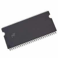
MT48LC64M8A2TG-75 IT:C Micron Technology Inc, MT48LC64M8A2TG-75 IT:C Datasheet - Page 29

MT48LC64M8A2TG-75 IT:C
Manufacturer Part Number
MT48LC64M8A2TG-75 IT:C
Description
DRAM Chip SDRAM 512M-Bit 64Mx8 3.3V 54-Pin TSOP-II Tray
Manufacturer
Micron Technology Inc
Type
SDRAMr
Datasheet
1.MT48LC64M8A2TG-75C_TR.pdf
(68 pages)
Specifications of MT48LC64M8A2TG-75 IT:C
Package
54TSOP-II
Density
512 Mb
Address Bus Width
15 Bit
Operating Supply Voltage
3.3 V
Maximum Clock Rate
133 MHz
Maximum Random Access Time
6|5.4 ns
Operating Temperature
-40 to 85 °C
Format - Memory
RAM
Memory Type
SDRAM
Memory Size
512M (64M x 8)
Speed
133MHz
Interface
Parallel
Voltage - Supply
3 V ~ 3.6 V
Package / Case
54-TSOP II
Lead Free Status / RoHS Status
Contains lead / RoHS non-compliant
Figure 18:
Figure 19:
PDF: 09005aef809bf8f3/Source: 09005aef80818a4a
512MbSDRAM.fm - Rev. L 10/07 EN
WRITE Burst
WRITE-to-WRITE
Note:
Note:
COMMAND
Data for any WRITE burst may be truncated with a subsequent READ command, and
data for a fixed-length WRITE burst may be immediately followed by a READ command.
After the READ command is registered, the data inputs will be ignored, and WRITEs will
not be executed. An example is shown in Figure 21 on page 30. Data n + 1 is either the
last of a burst of two or the last desired of a longer burst.
COMMAND
ADDRESS
ADDRESS
BL = 2. DQM is LOW.
DQM is LOW. Each WRITE command may be to any bank.
CLK
CLK
DQ
DQ
Transitioning Data
WRITE
WRITE
BANK,
COL n
BANK,
COL n
D
T0
D
T0
n
IN
n
IN
Transitioning Data
n + 1
NOP
n + 1
NOP
D
T1
T1
D
IN
IN
29
Don’t Care
WRITE
BANK,
COL b
NOP
T2
T2
D
b
IN
Micron Technology, Inc., reserves the right to change products or specifications without notice.
Don’t Care
T3
NOP
512Mb: x4, x8, x16 SDRAM
©2000 Micron Technology, Inc. All rights reserved.
Operations


