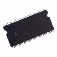
MT46V32M16P-5B:F Micron Technology Inc, MT46V32M16P-5B:F Datasheet - Page 61

MT46V32M16P-5B:F
Manufacturer Part Number
MT46V32M16P-5B:F
Description
DRAM Chip DDR SDRAM 512M-Bit 32Mx16 2.6V 66-Pin TSOP Tray
Manufacturer
Micron Technology Inc
Type
DDR SDRAMr
Datasheet
1.MT46V32M16P-5BF_TR.pdf
(91 pages)
Specifications of MT46V32M16P-5B:F
Density
512 Mb
Maximum Clock Rate
400 MHz
Package
66TSOP
Address Bus Width
15 Bit
Operating Supply Voltage
2.6 V
Maximum Random Access Time
0.7 ns
Operating Temperature
0 to 70 °C
Format - Memory
RAM
Memory Type
DDR SDRAM
Memory Size
512M (32Mx16)
Speed
5ns
Interface
Parallel
Voltage - Supply
2.5 V ~ 2.7 V
Package / Case
66-TSOP
Organization
32Mx16
Address Bus
15b
Access Time (max)
700ps
Operating Supply Voltage (typ)
2.6V
Package Type
TSOP
Operating Temp Range
0C to 70C
Operating Supply Voltage (max)
2.7V
Operating Supply Voltage (min)
2.5V
Supply Current
215mA
Pin Count
66
Mounting
Surface Mount
Operating Temperature Classification
Commercial
Lead Free Status / RoHS Status
Lead free / RoHS Compliant
Available stocks
Company
Part Number
Manufacturer
Quantity
Price
Company:
Part Number:
MT46V32M16P-5B:F
Manufacturer:
Micron
Quantity:
11 200
Company:
Part Number:
MT46V32M16P-5B:F
Manufacturer:
MICRON
Quantity:
20 000
Company:
Part Number:
MT46V32M16P-5B:F
Manufacturer:
MICRON
Quantity:
172
Part Number:
MT46V32M16P-5B:F
Manufacturer:
MICRON/美光
Quantity:
20 000
Company:
Part Number:
MT46V32M16P-5B:FTR
Manufacturer:
SONY
Quantity:
46
PDF: 09005aef80a1d9d4/Source: 09005aef82a95a3a
DDR_x4x8x16_Core2.fm - 512Mb DDR: Rev. N; Core DDR Rev. B 2/09 EN
Data from any READ burst may be truncated with a BURST TERMINATE command, as
shown in Figure 31 on page 66. The BURST TERMINATE latency is equal to the CL, that
is, the BURST TERMINATE command should be issued x cycles after the READ
command where x equals the number of desired data element pairs (pairs are required
by the 2n-prefetch architecture).
Data from any READ burst must be completed or truncated before a subsequent WRITE
command can be issued. If truncation is necessary, the BURST TERMINATE command
must be used, as shown in Figure 32 on page 67. The
t
defined in the section on WRITEs.) A READ burst may be followed by, or truncated with,
a PRECHARGE command to the same bank provided that auto precharge was not acti-
vated.
The PRECHARGE command should be issued x cycles after the READ command, where
x equals the number of desired data element pairs (pairs are required by the 2n-prefetch
architecture). This is shown in Figure 33 on page 68. Following the PRECHARGE
command, a subsequent command to the same bank cannot be issued until both
and
last data elements.
DQSS (MAX) case has a longer bus idle time. (
t
RP have been met. Part of the row precharge time is hidden during the access of the
61
Micron Technology, Inc., reserves the right to change products or specifications without notice.
t
512Mb: x4, x8, x16 DDR SDRAM
DQSS [MIN] and
t
DQSS (NOM) case is shown; the
©2000 Micron Technology, Inc. All rights reserved.
t
DQSS [MAX] are
Operations
t
RAS


