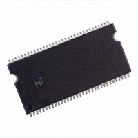
MT46V32M16P-5B:F Micron Technology Inc, MT46V32M16P-5B:F Datasheet - Page 79

MT46V32M16P-5B:F
Manufacturer Part Number
MT46V32M16P-5B:F
Description
DRAM Chip DDR SDRAM 512M-Bit 32Mx16 2.6V 66-Pin TSOP Tray
Manufacturer
Micron Technology Inc
Type
DDR SDRAMr
Datasheet
1.MT46V32M16P-5BF_TR.pdf
(91 pages)
Specifications of MT46V32M16P-5B:F
Density
512 Mb
Maximum Clock Rate
400 MHz
Package
66TSOP
Address Bus Width
15 Bit
Operating Supply Voltage
2.6 V
Maximum Random Access Time
0.7 ns
Operating Temperature
0 to 70 °C
Format - Memory
RAM
Memory Type
DDR SDRAM
Memory Size
512M (32Mx16)
Speed
5ns
Interface
Parallel
Voltage - Supply
2.5 V ~ 2.7 V
Package / Case
66-TSOP
Organization
32Mx16
Address Bus
15b
Access Time (max)
700ps
Operating Supply Voltage (typ)
2.6V
Package Type
TSOP
Operating Temp Range
0C to 70C
Operating Supply Voltage (max)
2.7V
Operating Supply Voltage (min)
2.5V
Supply Current
215mA
Pin Count
66
Mounting
Surface Mount
Operating Temperature Classification
Commercial
Lead Free Status / RoHS Status
Lead free / RoHS Compliant
Available stocks
Company
Part Number
Manufacturer
Quantity
Price
Company:
Part Number:
MT46V32M16P-5B:F
Manufacturer:
Micron
Quantity:
11 200
Company:
Part Number:
MT46V32M16P-5B:F
Manufacturer:
MICRON
Quantity:
20 000
Company:
Part Number:
MT46V32M16P-5B:F
Manufacturer:
MICRON
Quantity:
172
Part Number:
MT46V32M16P-5B:F
Manufacturer:
MICRON/美光
Quantity:
20 000
Company:
Part Number:
MT46V32M16P-5B:FTR
Manufacturer:
SONY
Quantity:
46
Figure 44:
PDF: 09005aef80a1d9d4/Source: 09005aef82a95a3a
DDR_x4x8x16_Core2.fm - 512Mb DDR: Rev. N; Core DDR Rev. B 2/09 EN
Command
t DQSS (NOM)
t DQSS (MIN)
t DQSS (MAX)
Address
DQS
DQS
DQS
CK#
DM
DM
DM
DQ
DQ
DQ
CK
WRITE-to-READ – Odd Number of Data, Interrupting
Notes:
Bank a,
WRITE
Col b
T0
t DQSS
t DQSS
t DQSS
1. DI b = data-in for column b; DO n = data-out for column n.
2. An interrupted burst of 4 is shown; one data element is written.
3.
4. A10 is LOW with the WRITE command (auto precharge is disabled).
5. DQS is required at T1n, T2, and T2n (nominal case) to register DM.
6. If the burst of 8 is used, DM and DQS are required at T3–T3n because the READ command
t
the last two data elements).
will not mask these data elements.
DI
b
WTR is referenced from the first positive CK edge after the last desired data-in pair (not
NOP
DI
T1
b
DI
b
T1n
NOP
T2
t WTR
T2n
79
Bank a,
READ
Col n
T3
T3n
Micron Technology, Inc., reserves the right to change products or specifications without notice.
CL = 2
CL = 2
CL = 2
NOP
T4
512Mb: x4, x8, x16 DDR SDRAM
Transitioning Data
T5
NOP
©2000 Micron Technology, Inc. All rights reserved.
DO
DO
DO
n
n
n
T5n
T6
NOP
Operations
Don’t Care
T6n


