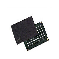
MT45W4MW16PCGA-70 IT Micron Technology Inc, MT45W4MW16PCGA-70 IT Datasheet - Page 10

MT45W4MW16PCGA-70 IT
Manufacturer Part Number
MT45W4MW16PCGA-70 IT
Description
Manufacturer
Micron Technology Inc
Datasheet
1.MT45W4MW16PCGA-70_IT.pdf
(23 pages)
Specifications of MT45W4MW16PCGA-70 IT
Operating Temperature (max)
85C
Operating Temperature (min)
-40C
Mounting
Surface Mount
Operating Temperature Classification
Industrial
Lead Free Status / RoHS Status
Compliant
Device Registers
Configuration Register (CR) Operation
Figure 9:
Partial-Array Refresh (CR[2:0]) Default = Full-Array Refresh
Table 3:
PDF: 09005aef81f0698d / Source: 09005aef81f06935
64mb_asyncpage_cr1_0_p25z.fm - Rev. D 7/09 EN
CR[2]
0
0
0
0
1
1
1
1
CR[7]
0
1
CR[1]
64Mb Address Patterns for PAR (CR[4] = 1)
Configuration Register Definition
0
0
1
1
0
0
1
1
All must be set to “0”
Page mode disabled (default)
Page mode enabled
Page Mode Enable/Disable
Reserved
A[21:8]
CR[0]
21–8
0
1
0
1
0
1
0
1
There are two registers on this device: the configuration register (CR) and the device ID
register (DIDR).
The CR defines how the CellularRAM device performs its transparent self refresh.
Altering the refresh parameters can dramatically reduce current consumption in
standby mode. Page mode control is also embedded in the CR. This register can be
updated any time the device is operating in a standby state. Figure 9 describes the
control bits used in the CR. At power-up, the CR is set to 0010h.
The PAR bits restrict refresh operation to a portion of the total memory array. This
feature allows the device to reduce standby current by refreshing only that part of the
memory array required by the host system. The refresh options are full array, one-half
array, one-quarter array, one-eighth array, or none of the array. The mapping of these
partitions can start at either the beginning or the end of the address map (see Table 3).
CR[4]
0
1
One-quarter of die
One-quarter of die
One-eighth of die
One-eighth of die
Active Section
Page
One-half of die
One-half of die
7
None of die
A7
DPD enabled
PAR enabled (default)
Setting is ignored
Sleep Mode
Full die
(Default 00b)
Reserved
6
A6
5
A5
Sleep
64Mb: 4 Meg x 16 Async/Page CellularRAM 1.0
A4
4
Must be set to “0”
10
Reserved
000000h–07FFFFh
000000h–3FFFFFh
000000h–1FFFFFh
000000h–0FFFFFh
200000h–3FFFFFh
300000h–3FFFFFh
380000h–3FFFFFh
Address Space
A3
3
Micron Technology, Inc., reserves the right to change products or specifications without notice.
0
CR[2]
A2
0
0
0
0
1
1
1
1
2
CR[1] CR[0]
0
0
1
1
0
0
1
1
PAR
1
A1
0
1
0
1
0
1
0
1
Full array (default)
Bottom 1/2 array
Bottom 1/4 array
Bottom 1/8 array
None of array
Top 1/2 array
Top 1/4 array
Top 1/8 array
PAR Refresh Coverage
4 Meg x 16
2 Meg x 16
1 Meg x 16
0 Meg x 16
2 Meg x 16
1 Meg x 16
512K x 16
512K x 16
A0
0
Size
©2005 Micron Technology, Inc. All rights reserved.
Device Registers
Address Bus
Configuration
Register
Density
64Mb
32Mb
16Mb
32Mb
16Mb
8Mb
0Mb
8Mb


