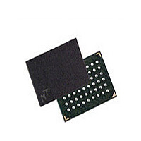
MT45W4MW16PCGA-70 IT Micron Technology Inc, MT45W4MW16PCGA-70 IT Datasheet - Page 16

MT45W4MW16PCGA-70 IT
Manufacturer Part Number
MT45W4MW16PCGA-70 IT
Description
Manufacturer
Micron Technology Inc
Datasheet
1.MT45W4MW16PCGA-70_IT.pdf
(23 pages)
Specifications of MT45W4MW16PCGA-70 IT
Operating Temperature (max)
85C
Operating Temperature (min)
-40C
Mounting
Surface Mount
Operating Temperature Classification
Industrial
Lead Free Status / RoHS Status
Compliant
Figure 13:
Table 9:
Table 10:
Figure 14:
Figure 15:
PDF: 09005aef81f0698d / Source: 09005aef81f06935
64mb_asyncpage_cr1_0_p25z.fm - Rev. D 7/09 EN
Description
Description
Deep power-down
Input capacitance
Input/output capacitance (DQ)
80
70
60
50
40
30
20
10
0
–40
Deep Power-Down Specifications
Capacitance
Typical Refresh Current vs. Temperature (I
–30
AC Input/Output Reference Waveform
AC Output Load Circuit
Notes:
Notes:
Notes:
–20
–10
1. Typical (TYP) I
1. These parameters are verified in device characterization and are not 100 percent tested.
Input
1. AC test inputs are driven at V
2. Input timing begins at V
3. Output timing ends at V
DUT
V
times (10 percent to 90 percent) < 1.6ns.
V
0
CC
SS
1
Q
Q
V
10
Temperature (°C)
CC
T
C
, V
V
V
= +25°C; f = 1 MHz;
CC
Test Point
IN
20
CC
Conditions
Conditions
Q/2
= V
Q = 1.95V; +85°C
ZZ
V
2
IN
CC
value applies across all operating temperatures and voltages.
30
= 0V
30pF
Q or 0V;
50Ω
40
CC
CC
64Mb: 4 Meg x 16 Async/Page CellularRAM 1.0
Q/2.
Q/2.
50
16
VccQ/2
CC
Q for a logic 1 and V
60
Test Points
TCR
Symbol
)
70
Symbol
Micron Technology, Inc., reserves the right to change products or specifications without notice.
I
ZZ
C
C
IN
IO
80
90
SS
100
Typ
Q for a logic 0. Input rise and fall
Min
2.0
3.5
3
Electrical Characteristics
V
CC
Q/2
©2005 Micron Technology, Inc. All rights reserved.
PAR = Full array
PAR = 1/2 of array
PAR = 1/4 of array
PAR = 1/8 of array
PAR = None of array
3
Output
Max
Max
10
6
6
Unit
Unit
µA
pF
pF


