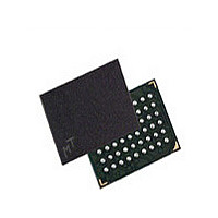
MT45W4MW16PCGA-70 IT Micron Technology Inc, MT45W4MW16PCGA-70 IT Datasheet - Page 3

MT45W4MW16PCGA-70 IT
Manufacturer Part Number
MT45W4MW16PCGA-70 IT
Description
Manufacturer
Micron Technology Inc
Datasheet
1.MT45W4MW16PCGA-70_IT.pdf
(23 pages)
Specifications of MT45W4MW16PCGA-70 IT
Operating Temperature (max)
85C
Operating Temperature (min)
-40C
Mounting
Surface Mount
Operating Temperature Classification
Industrial
Lead Free Status / RoHS Status
Compliant
Table 1:
Table 2:
PDF: 09005aef81f0698d / Source: 09005aef81f06935
64mb_asyncpage_cr1_0_p25z.fm - Rev. D 7/09 EN
Mode
Read
Write
Standby
No operation
Load configuration
register
Read configuration
register
PAR
DPD
G4, G3, H5, H4,
E3, H6, G2, H1,
H3, H2, D4, C4,
C3, B4, B3, A5,
D2, C2, C1, B1,
D3, E4, F4, F3,
G1, F1, F2, E2,
G6, F6, F5, E5,
D5, C6, C5, B6
Assignment
VFBGA
A4, A3
A6
A2
G5
A1
D6
D1
B5
B2
E1
E6
VFBGA Ball Descriptions
Bus Operations
DQ[15:0]
Symbol
A[21:0]
Notes:
V
V
WE#
OE#
UB#
ZZ#
CE#
LB#
V
V
CC
SS
CC
SS
Q
Q
Standby
Power
Active
Active
Active
Active
Active
1. When LB# and UB# are in select mode (LOW), DQ[15:0] are enabled. When only LB# is in
2. X = “Don’t Care.”
3. The device will consume active power in this mode whenever addresses are changed.
4. When the device is in standby mode, address inputs and data inputs/outputs are internally
5. V
6. DPD is initiated when CE# transitions from LOW to HIGH after writing CR[4] to 0. DPD is
DPD
Idle
output
Supply
Supply
Supply
Supply
Input/
Input
Input
Input
Input
Input
Input
Input
Type
select mode, DQ[7:0] are enabled. When only UB# is in the select mode, DQ[15:8] are
enabled.
isolated from any external influence.
rent.
maintained until CE# transitions from HIGH to LOW and is held LOW for
IN
= V
CC
Q or 0V; all device balls must be static (unswitched) in order to achieve standby cur-
Address inputs: Inputs for addresses during READ and WRITE operations.
Addresses are internally latched during READ and WRITE cycles. The address lines
are also used to define the value to be loaded into the CR.
Sleep enable: When ZZ# is LOW, the CR can be loaded or the device can enter one
of two low-power modes (DPD or PAR).
Chip enable: Activates the device when LOW. When CE# is HIGH, the device is
disabled and goes into standby or deep power-down mode.
Output enable: Enables the output buffers when LOW. When OE# is HIGH, the
output buffers are disabled.
Write enable: Determines if a given cycle is a WRITE cycle. If WE# is LOW, the cycle
is a WRITE to either a configuration register or to the memory array.
Lower byte enable: DQ[7:0].
Upper byte enable: DQ[15:8].
Data inputs/outputs.
Device power supply: (1.7–1.95V) Power supply for device core operation.
I/O power supply: (1.7–3.3V) Power supply for input/output buffers.
V
V
SS
SS
CE#
H
H
H
L
L
L
L
L
Q must be connected to ground.
must be connected to ground.
WE#
H
H
X
X
X
X
L
L
64Mb: 4 Meg x 16 Async/Page CellularRAM 1.0
3
OE#
X
X
X
X
X
X
L
L
2
Micron Technology, Inc., reserves the right to change products or specifications without notice.
LB#/UB#
Description
X
X
X
X
X
L
L
L
ZZ#
H
H
H
H
H
L
L
L
General Description
©2005 Micron Technology, Inc. All rights reserved.
Configuration
register out
DQ[15:0]
Data-out
Data-in
High-Z
High-Z
High-Z
High-Z
X
t
DPDX.
1
Notes
4, 5
3, 4
3
3
6


