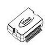
TLE6232GPNT Infineon Technologies, TLE6232GPNT Datasheet

TLE6232GPNT
Specifications of TLE6232GPNT
Related parts for TLE6232GPNT
TLE6232GPNT Summary of contents
Page 1
... Robotic Controls General description Six Channel Low-Side Switch in Smart Power Technology (SPT) with a Serial Peripheral Interface (SPI) and six open drain DMOS output stages. The TLE 6232 GP is pro- tected by embedded protection functions and designed for automotive and industrial applications. The output stages are controlled via an SPI Interface ...
Page 2
RESET GND VS PRG IN1 IN2 as Ch.1 IN3 as Ch.1 IN4 as Ch.1 IN5 as Ch.1 IN6 as Ch SPI Interface 16 bit SCLK CS V1 Detailed Block Diagram VS FAULT Normal function short to ground ...
Page 3
Pin Description Pin Symbol 1 GND Ground 2 NC not connected 3 OUT5 Power Output Channel not connected 5 OUT1 Power Output Channel 1 6 IN5 Input Channel 5 7 IN1 Input Channel Supply ...
Page 4
Maximum Ratings for T = – 40°C to 150°C j Parameter Supply Voltage Continuous Drain Source Voltage (OUT1...OUT8) Input Voltage, All Inputs and Data Lines Operating Temperature Range Storage Temperature Range Output Current per Channel (see el. characteristics) Single pulse ...
Page 5
... SO High State Output Voltage SO Low State Output Voltage Output Tri-state Leakage Current FAULT Output Low Voltage 2 For V < 4.5V the power stages are switched according the input signals and data bits or are definitely switched S off. This undervoltage reset gets active 25°C ...
Page 6
Electrical Characteristics cont. Parameter and Conditions V = 4 ° 150 °C ; Reset = (unless otherwise specified) 5. Diagnostic Functions Open Load Detection Voltage Short to ...
Page 7
... Description of the Power Stages 4 low side power switches for nominal currents (power stages OUT1 to OUT4). Con- trol is possible by input pins or via SPI. For T switches is below 500mΩ. 2 low side power switches for nominal currents up to 1.5A (power stages OUT5 and OUT6). ...
Page 8
... SPI control register Parallel Connection of Power Stages The power stages which are connected in parallel have to be switched on and off simultane- ously. In case of overload the ground current and the power dissipation are increasing. The applica- tion has to take into account that all maximum ratings are observed (e.g. operating tempera- ...
Page 9
... The data byte contains the input information for the eight channels. A logic high level at this pin (within the data byte) will switch on the power switch, provided that the corresponding parallel input is also switched on (AND-operation for channel 1 to 4). ...
Page 10
SPI Interface Power Stages 1...6 SCON_REG CS SCLK CS SCK SI Shift Register SO SPI Communication A SPI communication starts with a SPI instruction (SI control word) sent from the controller to TLE 6232 GP. Simultaneously the device sends the ...
Page 11
... If the 5V-reset (RESET) is active, the SPI output SO is switched into tristate. In order to increase the possible number of SPI participants on one and the same CS signal, bits 7 and 6 of the instruction byte are fixed as shown above. While receiving the first two bits of the instruction byte the data output SO has tristate ...
Page 12
Read back of SCON_REG (SCON bits and two high bits) - Read back of MUX_REG (MUX information for channel and two high bits) - Diagnostic information of channel bits ...
Page 13
Serial/Parallel Control of the Power Stages 1...6 (SPI-Instuctions: WR_MUX, RD_MUX, WR_SCON, RD_SCON) The following table shows the truth table for the control of the power stages 1...6. The register MUX_REG prescribes parallel or serial control of the power stages. The ...
Page 14
Description of the SPI Registers (SPI Instructions: RD_DIAG) Register: DIAG_REG1 7 6 ST7 ST6 State of FFH Reset: Access by Read only Controller: Bit Name 7-6 DIA4 5-4 DIA3 3-2 DIA2 1-0 DIA1 Note: This byte is always clocked out ...
Page 15
CS SCLK MSB Figure 2: Serial Interface Figure 3: Input Timing Diagram CS 0 SCKH t lead SCLK 0.7 V SCLK t valid SO ...
Page 16
... 80% 20% Figure 5: Power Outputs Timing is valid for resistive load with parallel and serial control. Rising edge of chip select initiates the switching Application Circuits µC e.g. C167 MTSR MRST CLK OFF V BB 10k VS PRG OUT1 FAULT OUT2 RESET IN1 TLE IN6 6232 GP ...
Page 17
... Parallel SPI Configuration Engine Management Application TLE 6232 GP in combination with TLE 6240 GP (16-fold switch) for relays and general pur- pose loads and TLE 6220 GP (quad switch) to drive the injector valves. This arrangement covers the numerous loads to be driven in a modern Engine Management/Powertrain system. ...
Page 18
Package and Ordering Code (all dimensions in mm) P-DSO 36-12 TLE 6232 GP Q67007A9397A702 V1 Ordering Code Page 18 Data Sheet TLE 6232 GP 24.Jan. 2002 ...
Page 19
... Infineon Technologies Components may only be used in life-support devices or systems with the express written approval of Infineon Technologies failure of such components can reasonably be expected to cause the failure of that life-support device or system affect the safety or effectiveness of that device or system. Life support devices or systems are in- tended to be implanted in the human body support and/or maintain and sustain and/or protect human life ...


