EP4CGX15BF14C8N Altera, EP4CGX15BF14C8N Datasheet - Page 174
EP4CGX15BF14C8N
Manufacturer Part Number
EP4CGX15BF14C8N
Description
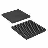
IC CYCLONE IV FPGA 15K 169FBGA
Manufacturer
Altera
Series
CYCLONE® IV GXr
Datasheets
1.EP4CGX15BN11C8N.pdf
(44 pages)
2.EP4CGX15BN11C8N.pdf
(14 pages)
3.EP4CGX15BN11C8N.pdf
(478 pages)
4.EP4CGX15BN11C8N.pdf
(10 pages)
Specifications of EP4CGX15BF14C8N
Number Of Logic Elements/cells
14400
Number Of Labs/clbs
900
Total Ram Bits
540000
Number Of I /o
72
Voltage - Supply
1.16 V ~ 1.24 V
Mounting Type
Surface Mount
Operating Temperature
0°C ~ 85°C
Package / Case
169-FBGA
Lead Free Status / RoHS Status
Lead free / RoHS Compliant
Number Of Gates
-
Other names
544-1475
Available stocks
Company
Part Number
Manufacturer
Quantity
Price
Company:

Part Number:
EP4CGX15BF14C8N
Manufacturer:
ALTERA33
Quantity:
276


8–8
Configuration Scheme
Table 8–3. Configuration Schemes for Cyclone IV GX Devices (EP4CGX15, EP4CGX22, and EP4CGX30 [except for F484
Package])
Table 8–4. Configuration Schemes for Cyclone IV GX Devices (EP4CGX30 [only for F484 package], EP4CGX50, EP4CGX75,
EP4CGX110, and EP4CGX150) (Part 1 of 2)
Cyclone IV Device Handbook, Volume 1
Notes to
(1) Configuration voltage standard applied to the V
(2) JTAG-based configuration takes precedence over other configuration schemes, which means the MSEL pin settings are ignored.
(3) Do not leave the MSEL pins floating. Connect them to V
JTAG-based configuration
Configuration Scheme
Altera recommends connecting the MSEL pins to GND if your device is only using JTAG configuration.
Configuration Scheme
Table
FPP
AS
PS
8–3:
AS
PS
1
A configuration scheme with different configuration voltage standards is selected by
driving the MSEL pins either high or low, as shown in
Table
Hardwire the MSEL pins to V
avoid problems detecting an incorrect configuration scheme. Do not drive the MSEL
pins with a microprocessor or another device.
(2)
8–5.
MSEL3 MSEL2 MSEL1 MSEL0
1
1
1
1
1
1
1
0
0
0
0
0
MSEL2
(3)
1
0
0
0
1
1
0
1
0
0
0
1
1
0
0
0
1
0
0
CCIO
MSEL1
supply of the bank in which the configuration pins reside.
(3)
0
1
0
1
0
1
0
CCA
0
1
0
1
0
1
0
0
1
0
0
1
or GND. These pins support the non-JTAG configuration scheme used in production.
Chapter 8: Configuration and Remote System Upgrades in Cyclone IV Devices
CCA
MSEL0
(3)
1
1
1
0
0
0
0
1
1
1
0
0
0
0
0
1
0
1
0
or GND without pull-up or pull-down resistors to
POR Delay
POR Delay
Standard
Standard
Standard
Standard
Standard
Standard
Standard
Standard
Standard
Fast
Fast
Fast
Fast
Fast
Fast
Fast
Fast
Fast
Fast
—
Configuration Voltage Standard (V)
Configuration Voltage Standard (V)
Table
© December 2010 Altera Corporation
8–3,
3.3, 3.0, 2.5
3.3, 3.0, 2.5
3.3, 3.0, 2.5
3.3, 3.0, 2.5
3.3, 3.0, 2.5
3.3, 3.0, 2.5
3.0, 2.5
3.0, 2.5
1.8, 1.5
Table
3.0, 2.5
3.0, 2.5
1.8, 1.5
1.8, 1.5
1.8, 1.5
1.8, 1.5
3.3
3.3
—
3.3
3.3
8–4, and
Configuration
(1)
(1)
Related parts for EP4CGX15BF14C8N
Image
Part Number
Description
Manufacturer
Datasheet
Request
R

Part Number:
Description:
CYCLONE II STARTER KIT EP2C20N
Manufacturer:
Altera
Datasheet:


Part Number:
Description:
CPLD, EP610 Family, ECMOS Process, 300 Gates, 16 Macro Cells, 16 Reg., 16 User I/Os, 5V Supply, 35 Speed Grade, 24DIP
Manufacturer:
Altera Corporation
Datasheet:
Part Number:
Description:
CPLD, EP610 Family, ECMOS Process, 300 Gates, 16 Macro Cells, 16 Reg., 16 User I/Os, 5V Supply, 15 Speed Grade, 24DIP
Manufacturer:
Altera Corporation
Datasheet:
Part Number:
Description:
Manufacturer:
Altera Corporation
Datasheet:
Part Number:
Description:
CPLD, EP610 Family, ECMOS Process, 300 Gates, 16 Macro Cells, 16 Reg., 16 User I/Os, 5V Supply, 30 Speed Grade, 24DIP
Manufacturer:
Altera Corporation
Datasheet:
Part Number:
Description:
High-performance, low-power erasable programmable logic devices with 8 macrocells, 10ns
Manufacturer:
Altera Corporation
Datasheet:
Part Number:
Description:
High-performance, low-power erasable programmable logic devices with 8 macrocells, 7ns
Manufacturer:
Altera Corporation
Datasheet:
Part Number:
Description:
Classic EPLD
Manufacturer:
Altera Corporation
Datasheet:
Part Number:
Description:
High-performance, low-power erasable programmable logic devices with 8 macrocells, 10ns
Manufacturer:
Altera Corporation
Datasheet:
Part Number:
Description:
Manufacturer:
Altera Corporation
Datasheet:
Part Number:
Description:
Manufacturer:
Altera Corporation
Datasheet:
Part Number:
Description:
Manufacturer:
Altera Corporation
Datasheet:
Part Number:
Description:
CPLD, EP610 Family, ECMOS Process, 300 Gates, 16 Macro Cells, 16 Reg., 16 User I/Os, 5V Supply, 25 Speed Grade, 24DIP
Manufacturer:
Altera Corporation
Datasheet: