EP4CGX15BF14C8N Altera, EP4CGX15BF14C8N Datasheet - Page 80
EP4CGX15BF14C8N
Manufacturer Part Number
EP4CGX15BF14C8N
Description
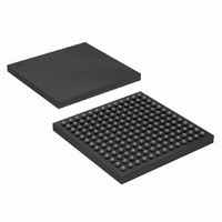
IC CYCLONE IV FPGA 15K 169FBGA
Manufacturer
Altera
Series
CYCLONE® IV GXr
Datasheets
1.EP4CGX15BN11C8N.pdf
(44 pages)
2.EP4CGX15BN11C8N.pdf
(14 pages)
3.EP4CGX15BN11C8N.pdf
(478 pages)
4.EP4CGX15BN11C8N.pdf
(10 pages)
Specifications of EP4CGX15BF14C8N
Number Of Logic Elements/cells
14400
Number Of Labs/clbs
900
Total Ram Bits
540000
Number Of I /o
72
Voltage - Supply
1.16 V ~ 1.24 V
Mounting Type
Surface Mount
Operating Temperature
0°C ~ 85°C
Package / Case
169-FBGA
Lead Free Status / RoHS Status
Lead free / RoHS Compliant
Number Of Gates
-
Other names
544-1475
Available stocks
Company
Part Number
Manufacturer
Quantity
Price
Company:

Part Number:
EP4CGX15BF14C8N
Manufacturer:
ALTERA33
Quantity:
276


5–18
Table 5–5. Cyclone IV GX PLL Features (Part 2 of 2)
Cyclone IV Device Handbook, Volume 1
PLL drives FREF for PPM detect
Notes to
(1) This is only applicable to EP4CGX50, EP4CGX75, EP4CGX110, and EP4CGX150 devices in F672 and F896 package.
(2) This is applicable to all Cyclone IV devices.
(3) This is applicable to all Cyclone IV devices except EP4CGX15 devices in all packages, EP4CGX22, and EP4CGX30 devices in F169 package.
(4) This is only applicable to EP4CGX15, EP4CGX22, and all EP4CGX30 devices except EP4CGX30 in the F484 package..
(5) C counters range from 1 through 512 if the output clock uses a 50% duty cycle. For any output clocks using a non-50% duty cycle, the post
(6) These clock pins can access the GCLK networks.
(7) These clock pins are only available in EP4CGX50, EP4CGX75, EP4CGX110, and EP4CGX150 devices and cannot access the GCLK networks.
(8) Only applicable if the input clock jitter is in the input jitter tolerance specifications.
(9) The smallest phase shift is determined by the voltage
(10) This is applicable to the EP4CGX30, EP4CGX50, EP4CGX75, EP4CGX110, and EP4CGX150 devices in F484 package.
range from 1 through 256.
CLK[17,19,20,21]p can be used as single-ended clock input pins.
can shift all output frequencies in increments of at least 45°. Smaller degree increments are possible depending on the frequency and divide parameters.
Table
5–5:
Features
Table 5–6
Table 5–6. Cyclone IV E PLL Features
C (output counters)
M, N, C counter sizes
Dedicated clock outputs
Clock input pins
Spread-spectrum input clock tracking
PLL cascading
Compensation modes
Phase shift resolution
Programmable duty cycle
Output counter cascading
Input clock switchover
User mode reconfiguration
Loss of lock detection
Notes to
(1) C counters range from 1 through 512 if the output clock uses a 50% duty cycle. For any output clocks using a
(2) Only applicable if the input clock jitter is in the input jitter tolerance specifications.
(3) The smallest phase shift is determined by the VCO period divided by eight. For degree increments, Cyclone IV E
non-50% duty cycle, the post-scale counters range from 1 through 256.
devices can shift all output frequencies in increments of at least 45°. Smaller degree increments are possible
depending on the frequency and divide parameters.
Table
lists the features available in Cyclone IV E PLLs.
Hardware Features
5–6:
(1),(10)
PLL_1
v
General Purpose PLLs
-
controlled oscillator (VCO) period divided by eight. For degree increments, Cyclone IV GX devices
(1),(10)
PLL_2
v
PLL_3
(2)
—
PLL_4
(3)
—
Chapter 5: Clock Networks and PLLs in Cyclone IV Devices
Mode, Normal Mode, and Zero Delay Buffer Mode
Source-Synchronous Mode, No Compensation
PLL_1
(4)
Availability
4 single-ended or 2 differential pairs
1 single-ended or 1 differential pair
Down to 96-ps increments
PLL_2
(4)
Through GCLK
© December 2010 Altera Corporation
Availability
1 to 512
v
Multipurpose PLLs
(1),(10)
PLL_5
v
v
v
v
v
5
(2)
PLLs in Cyclone IV Devices
(1)
v
(1),(10)
PLL_6
(3)
PLL_7
(1)
-
scale counters
PLL_8
(1)
Related parts for EP4CGX15BF14C8N
Image
Part Number
Description
Manufacturer
Datasheet
Request
R

Part Number:
Description:
CYCLONE II STARTER KIT EP2C20N
Manufacturer:
Altera
Datasheet:


Part Number:
Description:
CPLD, EP610 Family, ECMOS Process, 300 Gates, 16 Macro Cells, 16 Reg., 16 User I/Os, 5V Supply, 35 Speed Grade, 24DIP
Manufacturer:
Altera Corporation
Datasheet:
Part Number:
Description:
CPLD, EP610 Family, ECMOS Process, 300 Gates, 16 Macro Cells, 16 Reg., 16 User I/Os, 5V Supply, 15 Speed Grade, 24DIP
Manufacturer:
Altera Corporation
Datasheet:
Part Number:
Description:
Manufacturer:
Altera Corporation
Datasheet:
Part Number:
Description:
CPLD, EP610 Family, ECMOS Process, 300 Gates, 16 Macro Cells, 16 Reg., 16 User I/Os, 5V Supply, 30 Speed Grade, 24DIP
Manufacturer:
Altera Corporation
Datasheet:
Part Number:
Description:
High-performance, low-power erasable programmable logic devices with 8 macrocells, 10ns
Manufacturer:
Altera Corporation
Datasheet:
Part Number:
Description:
High-performance, low-power erasable programmable logic devices with 8 macrocells, 7ns
Manufacturer:
Altera Corporation
Datasheet:
Part Number:
Description:
Classic EPLD
Manufacturer:
Altera Corporation
Datasheet:
Part Number:
Description:
High-performance, low-power erasable programmable logic devices with 8 macrocells, 10ns
Manufacturer:
Altera Corporation
Datasheet:
Part Number:
Description:
Manufacturer:
Altera Corporation
Datasheet:
Part Number:
Description:
Manufacturer:
Altera Corporation
Datasheet:
Part Number:
Description:
Manufacturer:
Altera Corporation
Datasheet:
Part Number:
Description:
CPLD, EP610 Family, ECMOS Process, 300 Gates, 16 Macro Cells, 16 Reg., 16 User I/Os, 5V Supply, 25 Speed Grade, 24DIP
Manufacturer:
Altera Corporation
Datasheet: