EP4CGX15BF14C8N Altera, EP4CGX15BF14C8N Datasheet - Page 52
EP4CGX15BF14C8N
Manufacturer Part Number
EP4CGX15BF14C8N
Description
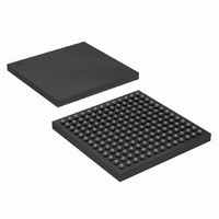
IC CYCLONE IV FPGA 15K 169FBGA
Manufacturer
Altera
Series
CYCLONE® IV GXr
Datasheets
1.EP4CGX15BN11C8N.pdf
(44 pages)
2.EP4CGX15BN11C8N.pdf
(14 pages)
3.EP4CGX15BN11C8N.pdf
(478 pages)
4.EP4CGX15BN11C8N.pdf
(10 pages)
Specifications of EP4CGX15BF14C8N
Number Of Logic Elements/cells
14400
Number Of Labs/clbs
900
Total Ram Bits
540000
Number Of I /o
72
Voltage - Supply
1.16 V ~ 1.24 V
Mounting Type
Surface Mount
Operating Temperature
0°C ~ 85°C
Package / Case
169-FBGA
Lead Free Status / RoHS Status
Lead free / RoHS Compliant
Number Of Gates
-
Other names
544-1475
Available stocks
Company
Part Number
Manufacturer
Quantity
Price
Company:

Part Number:
EP4CGX15BF14C8N
Manufacturer:
ALTERA33
Quantity:
276


3–16
Cyclone IV Device Handbook, Volume 1
Same-Port Read-During-Write Mode
This mode applies to a single-port RAM or the same port of a true dual-port RAM. In
the same port read-during-write mode, there are two output choices: New Data mode
(or flow-through) and Old Data mode. In New Data mode, new data is available on
the rising edge of the same clock cycle on which it was written. In Old Data mode, the
RAM outputs reflect the old data at that address before the write operation proceeds.
When using New Data mode together with byteena, you can control the output of
the RAM. When byteena is high, the data written into the memory passes to the
output (flow-through). When byteena is low, the masked-off data is not written into
the memory and the old data in the memory appears on the outputs. Therefore, the
output can be a combination of new and old data determined by byteena.
Figure 3–14
read-during-write behavior with both New Data and Old Data modes, respectively.
Figure 3–14. Same Port Read-During Write: New Data Mode
Figure 3–15. Same Port Read-During-Write: Old Data Mode
q_a (asynch)
q_a (asynch)
address_a
address_a
wren_a
wren_a
data_a
rden_a
rden_a
data_a
clk_a
clk_a
and
Figure 3–15
A
A
a0(old data)
show sample functional waveforms of same port
A
a0
B
a0
B
A
B
C
C
B
C
Chapter 3: Memory Blocks in Cyclone IV Devices
D
D
a1(old data)
D
© November 2009 Altera Corporation
a1
a1
E
E
D
E
Design Considerations
F
F
E
F
Related parts for EP4CGX15BF14C8N
Image
Part Number
Description
Manufacturer
Datasheet
Request
R

Part Number:
Description:
CYCLONE II STARTER KIT EP2C20N
Manufacturer:
Altera
Datasheet:


Part Number:
Description:
CPLD, EP610 Family, ECMOS Process, 300 Gates, 16 Macro Cells, 16 Reg., 16 User I/Os, 5V Supply, 35 Speed Grade, 24DIP
Manufacturer:
Altera Corporation
Datasheet:
Part Number:
Description:
CPLD, EP610 Family, ECMOS Process, 300 Gates, 16 Macro Cells, 16 Reg., 16 User I/Os, 5V Supply, 15 Speed Grade, 24DIP
Manufacturer:
Altera Corporation
Datasheet:
Part Number:
Description:
Manufacturer:
Altera Corporation
Datasheet:
Part Number:
Description:
CPLD, EP610 Family, ECMOS Process, 300 Gates, 16 Macro Cells, 16 Reg., 16 User I/Os, 5V Supply, 30 Speed Grade, 24DIP
Manufacturer:
Altera Corporation
Datasheet:
Part Number:
Description:
High-performance, low-power erasable programmable logic devices with 8 macrocells, 10ns
Manufacturer:
Altera Corporation
Datasheet:
Part Number:
Description:
High-performance, low-power erasable programmable logic devices with 8 macrocells, 7ns
Manufacturer:
Altera Corporation
Datasheet:
Part Number:
Description:
Classic EPLD
Manufacturer:
Altera Corporation
Datasheet:
Part Number:
Description:
High-performance, low-power erasable programmable logic devices with 8 macrocells, 10ns
Manufacturer:
Altera Corporation
Datasheet:
Part Number:
Description:
Manufacturer:
Altera Corporation
Datasheet:
Part Number:
Description:
Manufacturer:
Altera Corporation
Datasheet:
Part Number:
Description:
Manufacturer:
Altera Corporation
Datasheet:
Part Number:
Description:
CPLD, EP610 Family, ECMOS Process, 300 Gates, 16 Macro Cells, 16 Reg., 16 User I/Os, 5V Supply, 25 Speed Grade, 24DIP
Manufacturer:
Altera Corporation
Datasheet: