EP4CGX15BF14C8N Altera, EP4CGX15BF14C8N Datasheet - Page 188
EP4CGX15BF14C8N
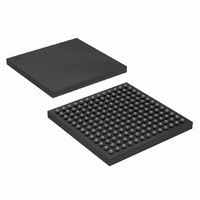
Manufacturer Part Number
EP4CGX15BF14C8N
Description
IC CYCLONE IV FPGA 15K 169FBGA
Manufacturer
Altera
Series
CYCLONE® IV GXr
Datasheets
1.EP4CGX15BN11C8N.pdf
(44 pages)
2.EP4CGX15BN11C8N.pdf
(14 pages)
3.EP4CGX15BN11C8N.pdf
(478 pages)
4.EP4CGX15BN11C8N.pdf
(10 pages)
Specifications of EP4CGX15BF14C8N
Number Of Logic Elements/cells
14400
Number Of Labs/clbs
900
Total Ram Bits
540000
Number Of I /o
72
Voltage - Supply
1.16 V ~ 1.24 V
Mounting Type
Surface Mount
Operating Temperature
0°C ~ 85°C
Package / Case
169-FBGA
Lead Free Status / RoHS Status
Lead free / RoHS Compliant
Number Of Gates
-
Other names
544-1475
Available stocks
Company
Part Number
Manufacturer
Quantity
Price
Company:

Part Number:
EP4CGX15BF14C8N
Manufacturer:
ALTERA33
Quantity:
276


8–22
Cyclone IV Device Handbook, Volume 1
f
For more information about the operation of the Numonyx StrataFlash Embedded
Memory P30 and P33 flash memories, search for the keyword “P30” or “P33” on the
Numonyx website (www.numonyx.com) to obtain the P30 or P33 family datasheet.
Single-Device AP Configuration
The following groups of interface pins are supported in Numonyx P30 and P33 flash
memories:
■
■
■
The following control signals are from the supported parallel flash memories:
■
■
■
■
■
■
The supported parallel flash memories output a control signal (WAIT) to Cyclone IV E
devices to indicate when synchronous data is ready on the data bus. Cyclone IV E
devices have a 24-bit address bus connecting to the address bus (A[24:1]) of the
flash memory. A 16-bit bidirectional data bus (DATA[15..0]) provides data transfer
between the Cyclone IV E device and the flash memory.
The following control signals are from the Cyclone IV E device to flash memory:
■
■
■
■
■
■
Control pins
Address pins
Data pins
CLK
active-low reset (RST#)
active-low chip enable (CE#)
active-low output enable (OE#)
active-low address valid (ADV#)
active-low write enable (WE#)
DCLK
active-low hard rest (nRESET)
active-low chip enable (FLASH_nCE)
active-low output enable for the DATA[15..0] bus and WAIT pin (nOE)
active-low address valid signal and is used to write data into the flash (nAVD)
active-low write enable and is used to write data into the flash (nWE)
Chapter 8: Configuration and Remote System Upgrades in Cyclone IV Devices
© December 2010 Altera Corporation
Configuration
Related parts for EP4CGX15BF14C8N
Image
Part Number
Description
Manufacturer
Datasheet
Request
R

Part Number:
Description:
CYCLONE II STARTER KIT EP2C20N
Manufacturer:
Altera
Datasheet:


Part Number:
Description:
CPLD, EP610 Family, ECMOS Process, 300 Gates, 16 Macro Cells, 16 Reg., 16 User I/Os, 5V Supply, 35 Speed Grade, 24DIP
Manufacturer:
Altera Corporation
Datasheet:
Part Number:
Description:
CPLD, EP610 Family, ECMOS Process, 300 Gates, 16 Macro Cells, 16 Reg., 16 User I/Os, 5V Supply, 15 Speed Grade, 24DIP
Manufacturer:
Altera Corporation
Datasheet:
Part Number:
Description:
Manufacturer:
Altera Corporation
Datasheet:
Part Number:
Description:
CPLD, EP610 Family, ECMOS Process, 300 Gates, 16 Macro Cells, 16 Reg., 16 User I/Os, 5V Supply, 30 Speed Grade, 24DIP
Manufacturer:
Altera Corporation
Datasheet:
Part Number:
Description:
High-performance, low-power erasable programmable logic devices with 8 macrocells, 10ns
Manufacturer:
Altera Corporation
Datasheet:
Part Number:
Description:
High-performance, low-power erasable programmable logic devices with 8 macrocells, 7ns
Manufacturer:
Altera Corporation
Datasheet:
Part Number:
Description:
Classic EPLD
Manufacturer:
Altera Corporation
Datasheet:
Part Number:
Description:
High-performance, low-power erasable programmable logic devices with 8 macrocells, 10ns
Manufacturer:
Altera Corporation
Datasheet:
Part Number:
Description:
Manufacturer:
Altera Corporation
Datasheet:
Part Number:
Description:
Manufacturer:
Altera Corporation
Datasheet:
Part Number:
Description:
Manufacturer:
Altera Corporation
Datasheet:
Part Number:
Description:
CPLD, EP610 Family, ECMOS Process, 300 Gates, 16 Macro Cells, 16 Reg., 16 User I/Os, 5V Supply, 25 Speed Grade, 24DIP
Manufacturer:
Altera Corporation
Datasheet: