FMS7401LVN14 Fairchild Semiconductor, FMS7401LVN14 Datasheet - Page 32
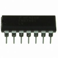
FMS7401LVN14
Manufacturer Part Number
FMS7401LVN14
Description
IC CTRLR POWER DGTL EEPROM 14DIP
Manufacturer
Fairchild Semiconductor
Datasheet
1.FMS7401LVN.pdf
(81 pages)
Specifications of FMS7401LVN14
Applications
Digital Power Controller
Core Processor
8-Bit
Program Memory Type
EEPROM (1 kB)
Ram Size
64 x 8
Number Of I /o
8
Voltage - Supply
2.7 V ~ 3.6 V
Operating Temperature
-40°C ~ 125°C
Mounting Type
Through Hole
Package / Case
14-DIP (0.300", 7.62mm)
Output Current
5 mA
Input Voltage
2.7 V to 3.6 V
Switching Frequency
2 MHz
Operating Temperature Range
- 40 C to + 125 C
Mounting Style
Through Hole
Lead Free Status / RoHS Status
Lead free / RoHS Compliant
Interface
-
Controller Series
-
Lead Free Status / Rohs Status
Lead free / RoHS Compliant
Other names
FMS7401LVN14_NL
FMS7401LVN14_NL
FMS7401LVN14_NL


FMS7401L
PRODUCT SPECIFICATION
6
PWM Timer 1 Circuit
The Pulse Width Modulation (PWM) Timer 1 circuit, a programmable 12-bit PWM timer with a 3-bit prescaler can be config-
ured to operate in both PWM and Input Capture Modes. In PWM Mode, the Timer 1 circuit may be configured to generate
pulses of a specified duty cycle and period on the T1HS1 (G0), T1HS2 (G5), and/or ADSTROBE (G1) timer output ports. On
the other hand, in Input Capture Mode, the Timer 1 circuit may be configured to capture and store the current timer value at the
time of a trigger defined by the rising or falling edge of the T1HS2 (G5) input port. In addition, the T1HS1 and ADSTROBE
PWM outputs may be generated as in the PWM Mode.
The Timer 1 circuit backbone is a 12-bit programmable up-counter (TMR1) that is accessible by software, with read-only
1
access, through the 4-bit TMR1HI and 8-bit TMR1LO memory mapped registers where TMR1={TMR1HI, TMR1LO}.
Upon
a system reset or once entering a new Timer 1 mode of operation, the 12-bit TMR1 counter is initialized to 0x000. Once a
selected Timer 1 mode is enabled, the TMR1 counter will begin incrementing by the F
clock with the programmed divide
T1CLK
factor defined by a 3-bit prescaler. Once the TMR1 overflows, TMR1 is reinitialized to 0x000 and resumes incrementing until
software disables the mode. In PWM Mode, the TMR1 overflow value may be programmed by software where, in Input
Capture Mode, the TMR1 will overflow once the 0xFFF count completes. The Timer 1 circuit may be programmed to generate
microcontroller hardware interrupts with every TMR1 overflow and capture.
The Timer 1 F
clock may be programmed to operate from high to low frequencies with the use of the programmable
T1CLK
digital clock multiplier (PLL) and internal oscillator in order to provide the maximum flexibility for various PWM applica-
tions.
6.1
PWM Timer 1 Configuration Registers
1
Software must access the six memory mapped PWM Timer 1 registers to configure and control the Timer 1 circuit.
The 8-bit
Prescale (PSCALE) register is used to configure the entire FMS7401L clock structure including the Timer 1’s F
. The 12-
T1CLK
bit Timer 1 Compare A (T1CMPA), Timer 1 Compare B (T1CMPB), and Timer 1 Reload (T1RA) registers are used to define
the PWM output signal’s duty cycle and period. The 5-bit Dead Time (DTIME) register is used to define the time delay (T
)
DT
between the PWM T1HS1 and T1HS2 edge transitions while in PWM Mode. The Timer 1 Control (T1CNTRL) register is used
to select Timer 1’s operating mode, enable its PWM output signals, and control its hardware interrupt (TMRI1).
6.1.1 PSCALE Register and Timer 1 Clock Configuration
Although the PSCALE register is part of the PWM Timer 1 circuit, its register bits configure the clock structure for the entire
FMS7401L along with the Timer 1 clock (F
). Refer to the
Clock Circuit
section of the datasheet for details regarding the
T1CLK
device’s clock structure. The F
source may be supplied by either the programmable F
PLL output or the main
T1CLK
PWMCLK
instruction (F
) clock. Once the F
source is selected, it may not be changed while the Timer 1 circuit is in PWM mode
ICLK
T1CLK
and running or in Input Capture Mode (run mode). Upon a system reset, the PSCALE register is automatically initialized to
0x00.
Bit 7 of the PSCALE register is the PLL circuit enable (PLLEN) bit. Before using any of the PLL outputs, software must
enable the PLL circuit and wait the T
to ensure that the PLL is locked into its appropriate frequency and in phase. The
PLL_LOCK
PLLEN bit may not be changed while the Timer 1 circuit is in run mode. Any attempts to write to PLLEN under this condition
will be ignored and its value will remain unchanged.
Bits 6 and 5 (FS[1:0]) of the PSCALE register are the bits used to select between the different output frequencies available to
the PLL’s F
output signal. FS selects between the four available PLL divide factors (divide-by-1/2/4/8) selecting an out-
PWMCLK
put frequency of 8/16/32/64MHz (see
Table
13). The FS bits may be changed by software at any time; however, if the Timer 1
circuit is in run mode, the FS value will not change the F
output frequency until after the TMR1 counter overflows end-
PWMCLK
ing the current PWM cycle. The last FS value at the TMR1 counter overflow will dictate the divide factor of the F
out-
PWMCLK
put for the next PWM cycle. When reading FS, the value reported will be the last value written by software and may not
necessarily reflect the divide factor for the current PWM cycle.
32
REV. 1.0.3 1/24/05
Related parts for FMS7401LVN14
Image
Part Number
Description
Manufacturer
Datasheet
Request
R

Part Number:
Description:
Digital Power Controller
Manufacturer:
Fairchild Semiconductor
Datasheet:
Part Number:
Description:
Digital Power Controller
Manufacturer:
Fairchild Semiconductor
Datasheet:
Part Number:
Description:
Fairchild Semiconductor [IGBT MODULE]
Manufacturer:
Fairchild Semiconductor
Datasheet:

Part Number:
Description:
Discrete Semiconductor Modules
Manufacturer:
Fairchild Semiconductor
Part Number:
Description:
Discrete Semiconductor Modules
Manufacturer:
Fairchild Semiconductor
Part Number:
Description:
This N-Channel MOSFET is produced using Fairchild Semiconductor’s advanced Power Trench® process
Manufacturer:
Fairchild Semiconductor
Datasheet:
Part Number:
Description:
This N-Channel MOSFET is produced using Fairchild Semiconductor’s advanced Power Trench® process
Manufacturer:
Fairchild Semiconductor
Datasheet:
Part Number:
Description:
This N-Channel MOSFET is produced using Fairchild Semiconductor’s advanced PowerTrench® process
Manufacturer:
Fairchild Semiconductor
Datasheet:
Part Number:
Description:
This N-Channel MOSFET is produced using Fairchild Semiconductor’s advanced PowerTrench® process
Manufacturer:
Fairchild Semiconductor
Datasheet:
Part Number:
Description:
This N-Channel MOSFET is produced using Fairchild Semiconductor’s advanced Power Trench® process
Manufacturer:
Fairchild Semiconductor
Datasheet:
Part Number:
Description:
This N-Channel logic Level MOSFETs are produced using Fairchild Semiconductor‘s advanced Power Trench® process that has been special tailored to minimize the on-state resistance and yet maintain superior switching performance
Manufacturer:
Fairchild Semiconductor
Datasheet:
Part Number:
Description:
This N-Channel MOSFET is produced using Fairchild Semiconductor’s advanced Power Trench® process
Manufacturer:
Fairchild Semiconductor
Datasheet:
Part Number:
Description:
This N-Channel SyncFET™ is produced using Fairchild Semiconductor’s advanced PowerTrench® process
Manufacturer:
Fairchild Semiconductor
Datasheet:
Part Number:
Description:
This N-Channel SyncFET™ is produced using Fairchild Semiconductor’s advanced PowerTrench® process
Manufacturer:
Fairchild Semiconductor
Datasheet:
Part Number:
Description:
This N-Channel SyncFET™ is produced using Fairchild Semiconductor’s advanced PowerTrench® process
Manufacturer:
Fairchild Semiconductor
Datasheet: