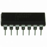
FMS7401LVN14 Fairchild Semiconductor, FMS7401LVN14 Datasheet - Page 61

FMS7401LVN14
Manufacturer Part Number
FMS7401LVN14
Description
IC CTRLR POWER DGTL EEPROM 14DIP
Manufacturer
Fairchild Semiconductor
Datasheet
1.FMS7401LVN.pdf
(81 pages)
Specifications of FMS7401LVN14
Applications
Digital Power Controller
Core Processor
8-Bit
Program Memory Type
EEPROM (1 kB)
Ram Size
64 x 8
Number Of I /o
8
Voltage - Supply
2.7 V ~ 3.6 V
Operating Temperature
-40°C ~ 125°C
Mounting Type
Through Hole
Package / Case
14-DIP (0.300", 7.62mm)
Output Current
5 mA
Input Voltage
2.7 V to 3.6 V
Switching Frequency
2 MHz
Operating Temperature Range
- 40 C to + 125 C
Mounting Style
Through Hole
Lead Free Status / RoHS Status
Lead free / RoHS Compliant
Interface
-
Controller Series
-
Lead Free Status / Rohs Status
Lead free / RoHS Compliant
Other names
FMS7401LVN14_NL
FMS7401LVN14_NL
FMS7401LVN14_NL
FMS7401L
between the device and external programmer hardware. The device sets SHIFT_OUT low during a page-write command by the
time the external programmer has issued the second rising edge of CLOCK informing the programmer that the memory write
is in progress. The external programmer must wait T
Vcc to initiate the next command cycle.
12.2.3 Byte Read Sequence
The external programmer can only perform memory reads a byte at a time. Before shifting each new command, the external
programmer must set the LOAD signal to Vcc. By definition, bit 31 of the command word must be shifted first followed by all
other bits. With each bit of the 32-bit read command word shifted, the device shifts out a bit of the 32-bit response word from
the previous command through the SHIFT_OUT pin. The external programmer must sample SHIFT_OUT after T
the rising edge of CLOCK. The serial response word sent immediately after entering programming mode may contain indeter-
minate data.
After all 32 bits of the read command word are shifted, the external programmer must set the LOAD signal to 0V and apply
two clock pulses to the CLOCK signal, as shown in
clock pulse, the data read from the address provided in the read command word is latched into the lower 8-bits of its response
word. Once LOAD is returned to Vcc, the next 32-bit command word may be shifted while the response word to the previous
read command is shifted out with the data read from memory. If the last read command has been shifted, a dummy read com-
mand must be shifted to collect the last response word containing the last data byte read.
Table 33. 32-Bit Command and Response Word
61
Bit 31
Bit 30
Bit 29
Bit 28
Bits 27 – 25
Bit 24
Bit 22
Bits 23, 21 – 18
Bits 17 – 8
Bits 7 – 0
Bit Number
Set to 1 to enable page mode memory access otherwise 0 for byte
mode.
Must be set to 0.
Set to 1 to access the data memory space (data EEPROM or
initialization registers) otherwise 0.
Set to 1 to access the code EEPROM otherwise 0.
Must be set to 0.
Set to 1 to perform a read or 0 to perform a write.
Set to 1 to perform a program memory erase otherwise 0.
Must be set to 0.
Lower 10-bits of the memory mapped address byte to read/write or
first byte of the page to write.
Data to be programmed if a write command or all zeros if a read
command.
Input Command Word
READY
Figure
for SHIFT_OUT to return high before returning the LOAD signal to
19, to complete the read cycle. At the rising edge of the second
Same as the input command word.
Same as the input command word.
Same as the input command word.
Same as the input command word.
Same as the input command word.
Same as the input command word.
Same as the input command word.
Same as the input command word.
Same as the input command word.
Same as the previous input write command word
or the data read after an input read command
word.
Output Response Word
PRODUCT SPECIFICATION
REV. 1.0.3 1/24/05
ACCESS
from


