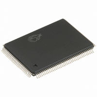
CY7C64713-128AXC Cypress Semiconductor Corp, CY7C64713-128AXC Datasheet - Page 18

CY7C64713-128AXC
Manufacturer Part Number
CY7C64713-128AXC
Description
IC MCU USB EZ FX1 16KB 128LQFP
Manufacturer
Cypress Semiconductor Corp
Series
EZ-USB FX1™r
Datasheet
1.CY7C64713-56LTXC.pdf
(55 pages)
Specifications of CY7C64713-128AXC
Program Memory Type
ROMless
Package / Case
128-LQFP
Applications
USB Microcontroller
Core Processor
8051
Controller Series
CY7C647xx
Ram Size
16K x 8
Interface
I²C, USB, USART
Number Of I /o
40
Voltage - Supply
3.15 V ~ 3.45 V
Operating Temperature
0°C ~ 70°C
Mounting Type
Surface Mount
Processor Series
CY7C64xx
Core
M8C
Data Bus Width
8 bit
Data Ram Size
16 KB
Interface Type
I2C/USART
Maximum Clock Frequency
48 MHz
Number Of Programmable I/os
40
Number Of Timers
3
Maximum Operating Temperature
+ 70 C
Mounting Style
SMD/SMT
Development Tools By Supplier
CY3674
Minimum Operating Temperature
0 C
Cpu Family
FX2LP
Device Core
8051
Device Core Size
8b
Frequency (max)
48MHz
Program Memory Size
Not Required
Total Internal Ram Size
16KB
# I/os (max)
40
Number Of Timers - General Purpose
3
Operating Supply Voltage (typ)
3.3V
Operating Supply Voltage (max)
3.45V
Operating Supply Voltage (min)
3.15V
Instruction Set Architecture
CISC
Operating Temp Range
0C to 70C
Operating Temperature Classification
Commercial
Mounting
Surface Mount
Pin Count
128
Package Type
TQFP
Controller Family/series
(8051) USB
Core Size
8 Bit
No. Of I/o's
40
Ram Memory Size
16KB
Cpu Speed
48MHz
No. Of Timers
3
Embedded Interface Type
I2C, SPI, UART, USB
Rohs Compliant
Yes
Lead Free Status / RoHS Status
Lead free / RoHS Compliant
For Use With
428-1681 - KIT USB FX1 DEVELOPMENT BOARD428-1677 - KIT DEVELOPMENT EZ-USB FX2LP428-1339 - KIT LOW SPEED PERSONALITY BOARD
Lead Free Status / Rohs Status
Compliant
Other names
428-1678
CY7C64713-128AXC
CY7C64713-128AXC
Available stocks
Company
Part Number
Manufacturer
Quantity
Price
Company:
Part Number:
CY7C64713-128AXC
Manufacturer:
CYPRESS
Quantity:
9 940
Company:
Part Number:
CY7C64713-128AXC
Manufacturer:
CYPRESS
Quantity:
513
Company:
Part Number:
CY7C64713-128AXC
Manufacturer:
Cypress Semiconductor Corp
Quantity:
10 000
Part Number:
CY7C64713-128AXC
Manufacturer:
CYPRESS/赛普拉斯
Quantity:
20 000
Table 8. FX1 Pin Definitions (continued)
Document #: 38-08039 Rev. *F
TQFP
Port A
128
99
35
12
11
82
83
84
85
89
90
1
TQFP
100
100
77
10
67
68
69
70
71
72
11
SSOP
56
49
12
40
41
42
43
44
45
11
5
QFN
56
42
54
33
34
35
36
37
38
5
4
RESET#
EA
XTALIN
XTALOUT
CLKOUT
PA0 or
INT0#
PA1 or
INT1#
PA2 or
SLOE
PA3 or
WU2
PA4 or
FIFOADR0
PA5 or
FIFOADR1
Name
Type
Input
Input
Input
Output
O/Z
I/O/Z
I/O/Z
I/O/Z
I/O/Z
I/O/Z
I/O/Z
Default
(PA0)
(PA1)
(PA2)
(PA3)
(PA4)
(PA5)
MHz
N/A
N/A
N/A
N/A
12
I
I
I
I
I
I
Active LOW Reset. Resets the entire chip. See the section
Wakeup”
External Access. This pin determines where the 8051 fetches code
between addresses 0x0000 and 0x3FFF. If EA = 0 the 8051 fetches
this code from its internal RAM. IF EA = 1 the 8051 fetches this code
from external memory.
Crystal Input. Connect this signal to a 24 MHz parallel-resonant,
fundamental mode crystal and load capacitor to GND.
It is also correct to drive the XTALIN with an external 24 MHz square
wave derived from another clock source. When driving from an external
source, the driving signal must be a 3.3V square wave.
Crystal Output. Connect this signal to a 24 MHz parallel-resonant,
fundamental mode crystal and load capacitor to GND.
If an external clock is used to drive XTALIN, leave this pin open.
CLKOUT: 12, 24 or 48 MHz clock, phase locked to the 24 MHz input
clock. The 8051 defaults to 12 MHz operation. The 8051 may
three-state this output by setting CPUCS.1 = 1.
Multiplexed pin whose function is selected by PORTACFG.0
PA0 is a bidirectional I/O port pin.
INT0# is the active-LOW 8051 INT0 interrupt input signal, which is
either edge triggered (IT0 = 1) or level triggered (IT0 = 0).
Multiplexed pin whose function is selected by:
PORTACFG.1
PA1 is a bidirectional I/O port pin.
INT1# is the active-LOW 8051 INT1 interrupt input signal, which is
either edge triggered (IT1 = 1) or level triggered (IT1 = 0).
Multiplexed pin whose function is selected by two bits:
IFCONFIG[1:0].
PA2 is a bidirectional I/O port pin.
SLOE is an input-only output enable with programmable polarity
(FIFOPINPOLAR.4) for the slave FIFOs connected to FD[7..0] or
FD[15..0].
Multiplexed pin whose function is selected by:
WAKEUP.7 and OEA.3
PA3 is a bidirectional I/O port pin.
WU2 is an alternate source for USB Wakeup, enabled by WU2EN bit
(WAKEUP.1) and polarity set by WU2POL (WAKEUP.4). If the 8051 is
in suspend and WU2EN = 1, a transition on this pin starts up the oscil-
lator and interrupts the 8051 to allow it to exit the suspend mode.
Asserting this pin inhibits the chip from suspending, if WU2EN = 1.
Multiplexed pin whose function is selected by:
IFCONFIG[1..0].
PA4 is a bidirectional I/O port pin.
FIFOADR0 is an input-only address select for the slave FIFOs
connected to FD[7..0] or FD[15..0].
Multiplexed pin whose function is selected by:
IFCONFIG[1..0].
PA5 is a bidirectional I/O port pin.
FIFOADR1 is an input-only address select for the slave FIFOs
connected to FD[7..0] or FD[15..0].
on page 6 for more details.
Description
CY7C64713
Page 18 of 55
“Reset and
[+] Feedback


