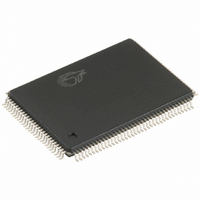
CY7C64713-128AXC Cypress Semiconductor Corp, CY7C64713-128AXC Datasheet - Page 44

CY7C64713-128AXC
Manufacturer Part Number
CY7C64713-128AXC
Description
IC MCU USB EZ FX1 16KB 128LQFP
Manufacturer
Cypress Semiconductor Corp
Series
EZ-USB FX1™r
Datasheet
1.CY7C64713-56LTXC.pdf
(55 pages)
Specifications of CY7C64713-128AXC
Program Memory Type
ROMless
Package / Case
128-LQFP
Applications
USB Microcontroller
Core Processor
8051
Controller Series
CY7C647xx
Ram Size
16K x 8
Interface
I²C, USB, USART
Number Of I /o
40
Voltage - Supply
3.15 V ~ 3.45 V
Operating Temperature
0°C ~ 70°C
Mounting Type
Surface Mount
Processor Series
CY7C64xx
Core
M8C
Data Bus Width
8 bit
Data Ram Size
16 KB
Interface Type
I2C/USART
Maximum Clock Frequency
48 MHz
Number Of Programmable I/os
40
Number Of Timers
3
Maximum Operating Temperature
+ 70 C
Mounting Style
SMD/SMT
Development Tools By Supplier
CY3674
Minimum Operating Temperature
0 C
Cpu Family
FX2LP
Device Core
8051
Device Core Size
8b
Frequency (max)
48MHz
Program Memory Size
Not Required
Total Internal Ram Size
16KB
# I/os (max)
40
Number Of Timers - General Purpose
3
Operating Supply Voltage (typ)
3.3V
Operating Supply Voltage (max)
3.45V
Operating Supply Voltage (min)
3.15V
Instruction Set Architecture
CISC
Operating Temp Range
0C to 70C
Operating Temperature Classification
Commercial
Mounting
Surface Mount
Pin Count
128
Package Type
TQFP
Controller Family/series
(8051) USB
Core Size
8 Bit
No. Of I/o's
40
Ram Memory Size
16KB
Cpu Speed
48MHz
No. Of Timers
3
Embedded Interface Type
I2C, SPI, UART, USB
Rohs Compliant
Yes
Lead Free Status / RoHS Status
Lead free / RoHS Compliant
For Use With
428-1681 - KIT USB FX1 DEVELOPMENT BOARD428-1677 - KIT DEVELOPMENT EZ-USB FX2LP428-1339 - KIT LOW SPEED PERSONALITY BOARD
Lead Free Status / Rohs Status
Compliant
Other names
428-1678
CY7C64713-128AXC
CY7C64713-128AXC
Available stocks
Company
Part Number
Manufacturer
Quantity
Price
Company:
Part Number:
CY7C64713-128AXC
Manufacturer:
CYPRESS
Quantity:
9 940
Company:
Part Number:
CY7C64713-128AXC
Manufacturer:
CYPRESS
Quantity:
513
Company:
Part Number:
CY7C64713-128AXC
Manufacturer:
Cypress Semiconductor Corp
Quantity:
10 000
Part Number:
CY7C64713-128AXC
Manufacturer:
CYPRESS/赛普拉斯
Quantity:
20 000
Sequence Diagram
Single and Burst Synchronous Read Example
Figure 30
signals during a synchronous FIFO read using IFCLK as the
synchronizing clock. This diagram illustrates a single read
followed by a burst read.
■
■
Document #: 38-08039 Rev. *F
Note t
running at 48 MHz, the FIFO address setup time is more than
one IFCLK cycle.
Note The data is pre-fetched and is driven on the bus when
SLOE is asserted.
At t = 0 the FIFO address is stable and the signal SLCS is
asserted (SLCS may be tied low in some applications).
At t = 1, SLOE is asserted. SLOE is an output enable only,
whose sole function is to drive the data bus. The data that is
driven on the bus is the data that the internal FIFO pointer is
currently pointing to. In this example it is the first data value in
the FIFO.
FIFO POINTER
FIFO DATA BUS
FLAGS
FIFOADR
SLRD
SLCS
DATA
IFCLK
SLOE
SFA
shows the timing relationship of the SLAVE FIFO
has a minimum of 25 ns. This means when IFCLK is
Not Driven
t=0
IFCLK
N
SLOE
Figure 30. Slave FIFO Synchronous Read Sequence and Timing Diagram
t=1
t
SFA
t
OEon
Figure 31. Slave FIFO Synchronous Sequence of Events Diagram
Data Driven: N
t=2
Driven: N
t
SRD
IFCLK
N
t
IFCLK
t
XFD
t=3
SLRD
t
RDH
t
XFLG
t
OEoff
N+1
t=4
N+1
IFCLK
t
N+1
FAH
SLOE
SLRD
Not Driven
IFCLK
N+1
t
T=0
SFA
■
■
The same sequence of events are shown for a burst read and
are marked with the time indicators of T = 0 through 5.
t
SLOE
OEon
At t = 2, SLRD is asserted. SLRD must meet the setup time of
t
the IFCLK) and maintain a minimum hold time of t
from the IFCLK edge to the deassertion of the SLRD signal).
If the SLCS signal is used, it must be asserted with SLRD, or
before SLRD is asserted (that is, the SLCS and SLRD signals
must both be asserted to start a valid read condition).
The FIFO pointer is updated on the rising edge of the IFCLK,
while SLRD is asserted. This starts the propagation of data
from the newly addressed location to the data bus. After a
propagation delay of t
IFCLK) the new data value is present. N is the first data value
read from the FIFO. To have data on the FIFO data bus, SLOE
MUST also be asserted.
SRD
T=2
>= t
T=1
N+1
N+1
IFCLK
(time from asserting the SLRD signal to the rising edge of
SRD
N+1
SLRD
t
XFD
N+2
N+2
IFCLK
N+2
N+3
N+3
IFCLK
XFD
t
XFD
(measured from the rising edge of
N+4
N+4
IFCLK
N+3
SLRD
t
>= t
XFD
N+4
N+4
RDH
IFCLK
t
N+4
OEoff
CY7C64713
SLOE
T=3
T=4
t
FAH
Page 44 of 55
Not Driven
RDH
IFCLK
N+4
(time
[+] Feedback


