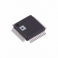
AD1986AJSTZ Analog Devices Inc, AD1986AJSTZ Datasheet - Page 50

AD1986AJSTZ
Manufacturer Part Number
AD1986AJSTZ
Description
IC CODEC HD AUDIO AC'97 48LQFP
Manufacturer
Analog Devices Inc
Series
SoundMAX®r
Type
Audio Codec '97, HDr
Datasheet
1.AD1986ABSTZ-REEL.pdf
(56 pages)
Specifications of AD1986AJSTZ
Data Interface
Serial
Resolution (bits)
20 b
Number Of Adcs / Dacs
2 / 6
Sigma Delta
No
Dynamic Range, Adcs / Dacs (db) Typ
85 / 91
Voltage - Supply, Analog
4.5 V ~ 5.5 V
Voltage - Supply, Digital
2.97 V ~ 3.63 V
Operating Temperature
0°C ~ 70°C
Mounting Type
Surface Mount
Package / Case
48-LQFP
Lead Free Status / RoHS Status
Lead free / RoHS Compliant
Available stocks
Company
Part Number
Manufacturer
Quantity
Price
Company:
Part Number:
AD1986AJSTZ
Manufacturer:
ADI
Quantity:
260
Part Number:
AD1986AJSTZ
Manufacturer:
ADI/亚德诺
Quantity:
20 000
Register
FIP (RO)
(Function
Information
Present)
IV
(Information
Valid Bit)
DL [4:0]
(Buffer
Delays,
Read/Write)
INV
(Inversion
Bit,
Read/Write,
Codec
Default)
AD1986A
INFORMATION AND I/O REGISTER (REGISTER 0x68, PAGE 01)
This address represents multiple registers (one for each supported function code (FC [3:0] bits (0x66 D [04:01])). These values are only
reset by power-on. It is used by the BIOS to store configuration information (per AC ’97 Revision 2.3 specifications) and must not be reset
by soft or hardware resets.
Reg
0x681
Table 114.
Name
Information
and I/O
Function
codec default. When set to a 1, this bit indicates that the G [4:0], INV, DL [4:0] (in Register 0x681), and ST [2:0] (in
Register 0x6A1) bits are supported and are read/write capable. This bit set to a 0 indicates that the G [4:0], INV, DL [4:0], and
ST [2:0] bits are not supported, and are read-only with a value of 0. Mono inputs and outputs report the relevant function
and sense information when T/R is set to 0 (tip). The FIP bit reports a 0 (Page 0x01, Register 0x68, Bit 0 reports no function
information present) when T/R is set to a 1 on a mono input or output.
FIP
0
1
Indicates whether a sensing method is provided by the codec and if information field is valid. This field is updated by the
codec.
IV
0
1
A number representing a delay measurement for the input and output channels. The default value is the delay internal to
the codec. The BIOS can add to this value the known delays external to the codec, such as for an external amplifier or logic.
Software will use this value to accurately calculate audio stream position with respect to what is been reproduced or
recorded. These values are in 20.83 microsecond (1/48000 second) units. For output channels, this timing is from the end of
AC link frame in which the sample is provided, until the time the analog signal appears at the output pin. For input streams,
this is from when the analog signal is presented at the pin until the representative sample is provided on the AC link. Analog
to analog paths are not considered in this measurement. The measurement is a typical measurement, at a 48 kHz sample
rate, with minimal in-codec processing (that is, 3D effects are turned off.) An example of an audio output delay is filter group
delay and FIFO or other sample buffers in the path. When an audio PCM sample is written to the codec in an AC ’97 frame it
will be delayed before the output pin is updated to that value.
DL [4:0]
0x00
0x01-0x1E
0x1F
Indicates that the codec presents a 180° phase shift to the signal. This bit is only reset by a power-on reset, since it is typically
written by the system BIOS and is not reset by codec hard or soft resets as long as power remains applied to the codec.
INV
0
1
D15
G4
Function
Function information not supported
Function information supported
Function
After codec reset de-assertion, it indicates the codec does not provide sensing logic and this bit will be read-
only. A completed sense cycle indicates that no information is provided on the sensing method.
After codec reset de-assertion, it indicates the codec provides sensing logic for this I/O and this bit is
read/write. After clearing this bit by writing 1, when a sense cycle is completed indicates that there is valid
information in the remaining descriptor bits. Writing 0 to this bit has no effect.
Function
Information not provided
Buffer delay: 20.83 µs per unit
Reserved
Function
No phase shift
Signal is shifted by 180° from the source signal
D14
G3
D13
G2
D12
G1
D11
G0
D10
INV
Rev. 0 | Page 50 of 56
D9
DL4
DL3
D8
D7
DL2
D6
DL1
DL0
D5
D4
IV
Power-on default
D3
x
x
D2
D1
x
D0
FIP
0xxxxx
Default


