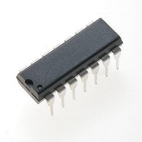
ML2004CP Fairchild Semiconductor, ML2004CP Datasheet - Page 8

ML2004CP
Manufacturer Part Number
ML2004CP
Description
Linear Regulators - Standard Gain/attenuator Logarithmic
Manufacturer
Fairchild Semiconductor
Datasheet
1.ML2004CP.pdf
(11 pages)
Specifications of ML2004CP
Input Voltage Max
3 V
Lead Free Status / Rohs Status
Lead free / RoHS Compliant
Available stocks
Company
Part Number
Manufacturer
Quantity
Price
Company:
Part Number:
ML2004CP
Manufacturer:
Fairchild Semiconductor
Quantity:
135
Part Number:
ML2004CP
Manufacturer:
MICRONLINEAR
Quantity:
20 000
ML2003, ML2004
Table 2. Coarse Gain Settings (F3-F0 = 0)
The device also has the capability to read out the data word
stored in the latch. This can be done by parallel loading the
data from the latch back into the shift register when the latch
signal, LATO, is high. The LATO pulse must occur when
SCK is low. Then, the data word can be shifted out of the
shift register serially to the output, SOD, on falling edges of
the shift clock, SCK.
8
C3 C2 C1 C0
0
0
0
0
0
0
0
0
1
1
1
1
1
1
1
1
LATO
0
0
0
0
1
1
1
1
0
0
0
0
1
1
1
1
SCK
SOD
LATI
SID
LATO
SOD
SCK
LATI
SID
0
0
1
1
0
0
1
1
0
0
1
1
0
0
1
1
0
1
0
1
0
1
0
1
0
1
0
1
0
1
0
1
ATTEN/GAIN = 1 ATTEN/GAIN = 0
-10.5
-12.0
-13.5
-15.0
-16.5
-18.0
-19.5
-21.0
-22.5
-1.5
-3.0
-4.5
-6.0
-7.5
-9.0
0
F0
0
Ideal Gain (dB)
F0
F1
1
0
F2
2
1
F1
Figure 10. Serial Mode Timing
10.5
12.0
13.5
15.0
16.5
18.0
19.5
21.0
22.5
1.5
3.0
4.5
6.0
7.5
9.0
0
F3
3
2
F2
b) READ
a) LOAD
C0
4
3
F3
The loading and reading of the data word can be done
continuously or in burst. Since the shift register and latch
circuitry inside the device is static, there are no minimum
frequency requirements on the clocks or data pulses.
However, there is coupling (typically less than 100µV) of
the digital signals into the analog section. This coupling
can be minimized by clocking the data bursts in during
noncritical intervals or at a frequency outside the analog
frequency range.
Parallel Mode
The parallel mode is selected by setting SER/PAR pin low.
The parallel interface allows the gain settings to be set with
external switches or from a parallel microprocessor inter-
face.
In parallel mode, the shift register and latch are bypassed and
connections are made directly to the gain select bits with
external pins ATTEN/GAIN, C3-C0, and F3-F0. Tables 1
and 2 describe how these pins program the gain. The pins
ATTEN/GAIN, C3-C0, and F3-F0 have internal pulldown
resistors to GND. The typical value of these pulldown
resistors is 100kΩ.
C1
5
C0
4
C2
6
C1
5
C3
7
C2
6
GAIN
ATT/
8
7
C3
GAIN
ATT/
8
PRODUCT SPECIFICATION
REV. 1.1.1 3/19/01


