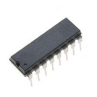
ML4802CP Fairchild Semiconductor, ML4802CP Datasheet - Page 8

ML4802CP
Manufacturer Part Number
ML4802CP
Description
Power Factor Correction ICs DIP-16
Manufacturer
Fairchild Semiconductor
Datasheet
1.ML4802CP.pdf
(15 pages)
Specifications of ML4802CP
Switching Frequency
212 KHz
Maximum Operating Temperature
+ 70 C
Mounting Style
Through Hole
Package / Case
PDIP-16
Minimum Operating Temperature
0 C
Lead Free Status / Rohs Status
Lead free / RoHS Compliant
Available stocks
Company
Part Number
Manufacturer
Quantity
Price
Part Number:
ML4802CP
Manufacturer:
ML
Quantity:
20 000
RAMP 1
ISENSE
VRMS
RT/CT
VFB
IAC
ML4802
control loop for the converter, which in turn drives a
current error amplifier and switching output driver. The
second requirement is met by using the rectified AC line
voltage to modulate the output of the voltage control
loop. Such modulation causes the current error amplifier
to command a power stage current which varies directly
with the input voltage. In order to prevent ripple which
will necessarily appear at the output of the boost circuit
(typically about 10VAC on a 385V DC level, or about
40VAC during Green Mode operation) from introducing
distortion back through the voltage error amplifier, the
bandwidth of the voltage loop is deliberately kept low. A
final refinement is to adjust the overall gain of the PFC
such to be proportional to 1/V
transfer function of the system as the AC input voltage
varies.
Since the boost converter topology in the ML4802 PFC is
of the current-averaging type, no slope compensation is
required.
8
FUNCTIONAL DESCRIPTION (Continued)
15
2
4
3
8
7
2.5V
+
-
VEA
MODULATOR
GAIN
VEAO
16
1.6k
IN
1.6k
2, which linearizes the
+
–
IEA
8V
IEAO
Figure 3. PFC Section Block Diagram
1
OSCILLATOR
DUTY CYCLE
LIMIT
POWER FACTOR CORRECTOR
CONTROLLER
÷2
PFC
PFC SECTION
Gain Modulator
Figure 3 shows a block diagram of the PFC section of the
ML4802. The gain modulator is the heart of the PFC, as it
is this circuit block which controls the response of the
current loop to line voltage waveform and frequency, rms
line voltage, and PFC output voltage. There are three
inputs to the gain modulator. These are:
1) A current representing the instantaneous input voltage
2) A voltage proportional to the long-term rms AC line
3) The output of the voltage error amplifier, VEAO. The
(amplitude and waveshape) to the PFC. The rectified
AC input sine wave is converted to a proportional
current via a resistor and is then fed into the gain
modulator at IAC. Sampling current in this way
minimizes ground noise, as is required in high power
switching power conversion environments. The gain
modulator responds linearly to this current.
voltage, derived from the rectified line voltage after
scaling and filtering. This signal is presented to the
gain modulator at VRMS. The gain modulator’s output
is inversely proportional to VRMS
low values of VRMS where special gain contouring
takes over to limit power dissipation of the circuit
components under heavy brownout conditions). The
relationship between VRMS and gain is designated as
K, and is illustrated in the Typical Performance
Characteristics.
gain modulator responds linearly to variations in this
voltage.
2.75V
-1V
+
+
-
-
PFC ILIMIT
OVP
GREEN MODE
CONTROLLER
FROM
OUTPUT
DRIVER
PFC
REFERENCE
2
REV. 1.0.1 12/12/2000
(except at unusually
VCC
7.5V
13
14
12
PFC OUT
VREF


