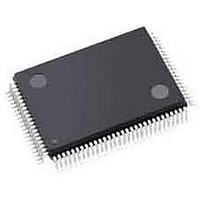
ispPAC-POWR1220AT8-01T100I Lattice, ispPAC-POWR1220AT8-01T100I Datasheet - Page 34

ispPAC-POWR1220AT8-01T100I
Manufacturer Part Number
ispPAC-POWR1220AT8-01T100I
Description
Supervisory Circuits Prec Prg Pwr Spply S eq. Mon. Mrg Trim I
Manufacturer
Lattice
Series
ispPAC®r
Datasheet
1.ISPPAC-POWR1220AT8-02TN100I.pdf
(54 pages)
Specifications of ispPAC-POWR1220AT8-01T100I
Number Of Voltages Monitored
12
Undervoltage Threshold
0.8 V
Output Type
Open Collector / Drain
Manual Reset
Not Resettable
Watchdog
No Watchdog
Power-up Reset Delay (typ)
500 ms
Supply Voltage (max)
3.96 V
Supply Voltage (min)
2.8 V
Supply Current (typ)
40 mA
Mounting Style
SMD/SMT
Package / Case
TQFP-100
Applications
General Purpose
Voltage - Input
-0.3 V ~ 5.9 V
Voltage - Supply
2.8 V ~ 3.96 V
Current - Supply
40mA
Operating Temperature
-40°C ~ 85°C
Mounting Type
*
Lead Free Status / Rohs Status
Lead free / RoHS Compliant
Available stocks
Company
Part Number
Manufacturer
Quantity
Price
Company:
Part Number:
ISPPAC-POWR1220AT8-01T100I
Manufacturer:
Lattice Semiconductor Corporation
Quantity:
10 000
Table 1-9. I
Lattice Semiconductor
Several registers are provided for monitoring the status of the analog inputs. The three registers
VMON_STATUS[0:2] provide the ability to read the status of the VMON output comparators. The ability to read
both the ‘a’ and ‘b’ comparators from each VMON input is provided through the VMON input registers. Note that if
a VMON input is configured to window comparison mode, then the corresponding VMONxA register bit will reflect
the status of the window comparison.
Figure 1-24. VMON Status Registers
It is also possible to directly read the value of the voltage present on any of the VMON inputs by using the ispPAC-
POWR1220AT8’s ADC. Three registers provide the I
Figure 1-25. ADC Interface Registers
To perform an A/D conversion, one must set the input attenuator and channel selector. Two input ranges may be
set using the attenuator, 0 - 2.048V and 0 - 6.144V. Table 1-10 shows the input attenuator settings.
1. “X” = Non-functional bit (bits read out as 1’s).
2. “–” = State depends on device configuration or input status.
Register Address
0x1A
0x19
2
C Control Registers (Cont.)
0x00 - VMON_STATUS0 (Read Only)
0x01 - VMON_STATUS1 (Read Only)
0x02 - VMON_STATUS2 (Read Only)
0x07 - ADC_VALUE_LOW (Read Only)
0x08 - ADC_VALUE_HIGH (Read Only)
0x09 - ADC_MUX (Read/Write)
VMON12B
VMON4B
VMON8B
Register Name
D11
b7
b7
b7
D3
b7
b7
b7
X
trim7_trim
trim8_trim
VMON12A
VMON4A
VMON8A
D10
b6
b6
b6
D2
b6
b6
b6
X
VMON11B
VMON3B
VMON7B
Read/Write
b5
b5
b5
D1
D9
b5
b5
b5
X
R/W
R/W
VMON11A
VMON3A
VMON7A
ATTEN
D0
D8
b4
b4
b4
b4
b4
b4
2
Trim DAC 7 [7:0]
Trim DAC 8 [7:0]
C interface to the ADC (Figure 1-24).
1-34
VMON10B
VMON2B
VMON6B
SEL3
D7
b3
b3
b3
b3
b3
b3
1
Description
VMON10A
VMON2A
VMON6A
ispPAC-POWR1220AT8 Data Sheet
SEL2
D6
b2
b2
b2
b2
b2
b2
1
VMON1B
VMON5B
VMON9B
SEL1
D5
b1
b1
b1
b1
b1
b1
1
VMON1A
VMON5A
VMON9A
DONE
SEL0
D4
b0
b0
b0
b0
b0
b0
Value After POR
1 0 0 0 0 0 0 0
1 0 0 0 0 0 0 0
1, 2


