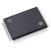
ispPAC-POWR1220AT8-01T100I Lattice, ispPAC-POWR1220AT8-01T100I Datasheet - Page 50

ispPAC-POWR1220AT8-01T100I
Manufacturer Part Number
ispPAC-POWR1220AT8-01T100I
Description
Supervisory Circuits Prec Prg Pwr Spply S eq. Mon. Mrg Trim I
Manufacturer
Lattice
Series
ispPAC®r
Datasheet
1.ISPPAC-POWR1220AT8-02TN100I.pdf
(54 pages)
Specifications of ispPAC-POWR1220AT8-01T100I
Number Of Voltages Monitored
12
Undervoltage Threshold
0.8 V
Output Type
Open Collector / Drain
Manual Reset
Not Resettable
Watchdog
No Watchdog
Power-up Reset Delay (typ)
500 ms
Supply Voltage (max)
3.96 V
Supply Voltage (min)
2.8 V
Supply Current (typ)
40 mA
Mounting Style
SMD/SMT
Package / Case
TQFP-100
Applications
General Purpose
Voltage - Input
-0.3 V ~ 5.9 V
Voltage - Supply
2.8 V ~ 3.96 V
Current - Supply
40mA
Operating Temperature
-40°C ~ 85°C
Mounting Type
*
Lead Free Status / Rohs Status
Lead free / RoHS Compliant
Available stocks
Company
Part Number
Manufacturer
Quantity
Price
Company:
Part Number:
ISPPAC-POWR1220AT8-01T100I
Manufacturer:
Lattice Semiconductor Corporation
Quantity:
10 000
Lattice Semiconductor
ispPAC-POWR1220AT8 Data Sheet
2
UES_PROGRAM – This instruction will program the content of the UES Register into the UES E
CMOS memory.
The device must already be in programming mode (PROGRAM_ENABLE instruction). This instruction also forces
the outputs into the OUTPUTS_HIGHZ.
ERASE_DONE_BIT – This instruction clears the 'Done' bit, which prevents the ispPAC-POWR1220AT8 sequence
from starting.
PROGRAM_DONE_BIT – This instruction sets the 'Done' bit, which enables the ispPAC-POWR1220AT8
sequence to start.
RESET – This instruction resets the PLD sequence and output macrocells.
IN1_RESET_JTAG_BIT – This instruction clears the JTAG Register logic input 'IN1.' The PLD input has to be con-
figured to take input from the JTAG Register in order for this command to have effect on the sequence.
IN1_SET_JTAG_BIT – This instruction sets the JTAG Register logic input 'IN1.' The PLD input has to be config-
ured to take input from the JTAG Register in order for this command to have effect on the sequence.
PLD_VERIFY_INCR – This instruction reads out the PLD data register for the current address and increments the
address register for the next read.
Notes:
In all of the descriptions above, OUTPUTS_HIGHZ refers both to the instruction and the state of the digital output
pins, in which the open-drains are tri-stated and the FET drivers are pulled low.
2
Before any of the above programming instructions are executed, the respective E
CMOS bits need to be erased
using the corresponding erase instruction.
1-50


