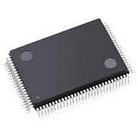
ispPAC-POWR1220AT8-01T100I Lattice, ispPAC-POWR1220AT8-01T100I Datasheet - Page 5

ispPAC-POWR1220AT8-01T100I
Manufacturer Part Number
ispPAC-POWR1220AT8-01T100I
Description
Supervisory Circuits Prec Prg Pwr Spply S eq. Mon. Mrg Trim I
Manufacturer
Lattice
Series
ispPAC®r
Datasheet
1.ISPPAC-POWR1220AT8-02TN100I.pdf
(54 pages)
Specifications of ispPAC-POWR1220AT8-01T100I
Number Of Voltages Monitored
12
Undervoltage Threshold
0.8 V
Output Type
Open Collector / Drain
Manual Reset
Not Resettable
Watchdog
No Watchdog
Power-up Reset Delay (typ)
500 ms
Supply Voltage (max)
3.96 V
Supply Voltage (min)
2.8 V
Supply Current (typ)
40 mA
Mounting Style
SMD/SMT
Package / Case
TQFP-100
Applications
General Purpose
Voltage - Input
-0.3 V ~ 5.9 V
Voltage - Supply
2.8 V ~ 3.96 V
Current - Supply
40mA
Operating Temperature
-40°C ~ 85°C
Mounting Type
*
Lead Free Status / Rohs Status
Lead free / RoHS Compliant
Available stocks
Company
Part Number
Manufacturer
Quantity
Price
Company:
Part Number:
ISPPAC-POWR1220AT8-01T100I
Manufacturer:
Lattice Semiconductor Corporation
Quantity:
10 000
Lattice Semiconductor
Pin Descriptions (Cont.)
1. [IN1...IN6] are inputs to the PLD. The thresholds for these pins are referenced by the voltage on VCCINP.
2. IN1 pin can also be controlled through JTAG interface.
3. [IN2..IN6] can also be controlled through I
4. The VMON inputs can be biased independently from VCCA. Unused VMONs should be tied to GNDD.
5. The VMONGS inputs are the ground sense line for each given VMON pin. The VMON input pins along with the VMONGS ground sense
6. Open-drain outputs require an external pull-up resistor to a supply.
7. VCCD and VCCA pins must be connected together on the circuit board.
8. GNDA and GNDD pins must be connected together on the circuit board.
9. The RESETb pin should only be used for cascading two or more ispPAC-POWR1220AT8 devices.
10. The VCCPROG pin MUST be left floating when VCCD and VCCA are powered.
81, 99, 100
26, 27, 29,
35, 41, 49,
76, 77, 78,
Number
44, 59
pins implement a differential pair for each voltage monitor to allow remote sense at the load. VMONGS lines must be connected and are
not to exceed -0.2V - +0.3V in reference to the GNDA pin.
73
91
95
96
34
37
28
31
30
32
92
93
TRIM8
RESETb
PLDCLK
MCLK
TDO
TCK
TMS
TDI
ATDI
TDISEL
SCL
SDA
RESERVED
NC
Name
9
Analog Output
Digital I/O
Digital Output
Digital I/O
Digital Output
Digital Input
Digital Input
Digital Input
Digital Input
Digital Input
Digital Input
Digital I/O
Pin Type
2
C/SMBus interface.
-320mV to +320mV
from Programmable
DAC Offset
0V to 3.96V
0V to 3.96V
0V to 3.96V
0V to 5.5V
0V to 5.5V
0V to 5.5V
0V to 5.5V
0V to 5.5V
0V to 5.5V
0V to 5.5V
0V to 5.5V
Voltage Range
1-5
ispPAC-POWR1220AT8 Data Sheet
Trim DAC Output 8
Device Reset (Active Low)
250kHz PLD Clock Output (Tristate), CMOS
Output
8MHz Clock I/O (Tristate), CMOS Drive
JTAG Test Data Out
JTAG Test Clock Input
JTAG Test Mode Select
JTAG Test Data In, TDISEL pin = 1
JTAG Test Data In (Alternate), TDISEL Pin = 0
Select TDI/ATDI Input
I
I
Reserved - Do Not Connect
No Internal Connection
2
2
C Serial Clock Input
C Serial Data, Bi-directional Pin
Description


