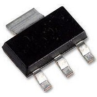
FDT86113LZ Fairchild Semiconductor, FDT86113LZ Datasheet - Page 2

FDT86113LZ
Manufacturer Part Number
FDT86113LZ
Description
MOSFET Power 100V N-Channel PowerTrench MOSFET
Manufacturer
Fairchild Semiconductor
Datasheet
1.FDT86113LZ.pdf
(6 pages)
Specifications of FDT86113LZ
Configuration
Single
Transistor Polarity
N-Channel
Resistance Drain-source Rds (on)
100 mOhms
Forward Transconductance Gfs (max / Min)
8 S
Drain-source Breakdown Voltage
100 V
Continuous Drain Current
3.3 A
Power Dissipation
2.2 W
Maximum Operating Temperature
+ 150 C
Mounting Style
SMD/SMT
Package / Case
SOT-223
Gate Charge Qg
4.1 nC
Minimum Operating Temperature
- 55 C
Lead Free Status / Rohs Status
Details
Available stocks
Company
Part Number
Manufacturer
Quantity
Price
Part Number:
FDT86113LZ
Manufacturer:
ON/安森美
Quantity:
20 000
FDT86113LZ Rev.C
Notes:
1. R
2. Pulse Test: Pulse Width < 300 Ps, Duty cycle < 2.0%.
3. Starting T
4. The diode connected between the gate and source serves only as protection against ESD. No gate overvoltage rating is implied.
Electrical Characteristics
Off Characteristics
On Characteristics
Dynamic Characteristics
Switching Characteristics
Drain-Source Diode Characteristics
BV
'BV
I
I
V
r
g
C
C
C
t
t
t
t
Q
Q
Q
Q
V
t
Q
DSS
GSS
'V
d(on)
r
d(off)
f
rr
DS(on)
FS
R
GS(th)
iss
oss
rss
SD
'T
'T
g
g
gs
gd
rr
Symbol
TJA
TJC
DSS
GS(th)
DSS
J
J
is the sum of the junction-to-case and case-to-ambient thermal resistance where the case thermal reference is defined as the solder mounting surface of the drain pins.
is guaranteed by design while R
J
= 25
°
Drain to Source Breakdown Voltage
Breakdown Voltage Temperature
Coefficient
Zero Gate Voltage Drain Current
Gate to Source Leakage Current
Gate to Source Threshold Voltage
Gate to Source Threshold Voltage
Temperature Coefficient
Static Drain to Source On Resistance
Forward Transconductance
Input Capacitance
Output Capacitance
Reverse Transfer Capacitance
Turn-On Delay Time
Rise Time
Turn-Off Delay Time
Fall Time
Total Gate Charge
Total Gate Charge
Gate to Source Gate Charge
Gate to Drain “Miller” Charge
Source to Drain Diode Forward Voltage
Reverse Recovery Time
Reverse Recovery Charge
C, L = 0.3 mH, I
(Note 2)
AS
= 8 A, V
TJA
Parameter
is determined by the user’s board design.
DD
= 90 V, V
a)
T
55 °C/W when mounted on a
1 in
J
= 25 °C unless otherwise noted
GS
2
pad of 2 oz copper
= 10 V.
V
V
V
V
V
f = 1 MHz
V
I
V
V
V
T
V
V
V
I
I
I
V
V
D
F
D
D
DD
GS
GS
GS
J
DS
GS
GS
GS
GS
DS
GS
GS
DS
GS
= 3.3 A, di/dt = 100 A/Ps
= 250 PA, referenced to 25 °C
= 250 PA, V
= 250 PA, referenced to 25 °C
= 125 °C
2
= 50 V, V
= 50 V, I
= 10 V, R
= 0 V to 10 V
= 0 V to 5 V
= 10 V, I
= 0 V, I
= 0 V, I
= 80 V, V
= V
= 10 V, I
= 4.5 V, I
= 10 V, I
= ±20 V, V
DS
Test Conditions
, I
S
S
D
D
D
D
D
= 1 A
= 3.3 A
D
GS
GEN
GS
= 250 PA
GS
= 3.3 A,
= 3.3 A
= 3.3 A,
= 3.3 A
DS
= 2.7 A
= 0 V,
= 0 V
= 0 V
= 0 V
= 6 :
V
I
D
DD
= 3.3 A
= 50 V,
(Note 2)
(Note 2)
b)
118 °C/W when mounted on
a minimum pad of 2 oz copper
Min
1.0
100
0.86
0.77
0.68
0.85
234
140
3.1
Typ
1.7
46
3.8
1.3
1.5
4.1
2.3
31
21
75
95
10
-5
71
8
Max
315
100
145
189
1.3
1.2
±10
2.5
65
6.8
3.9
49
34
10
10
20
10
5
www.fairchildsemi.com
1
mV/°C
mV/°C
Units
m:
nC
pF
pF
pF
PA
PA
nC
nC
nC
nC
ns
ns
ns
ns
ns
V
S
V
V


