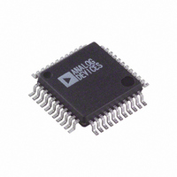
ADV7177KS-REEL Analog Devices Inc, ADV7177KS-REEL Datasheet - Page 25

ADV7177KS-REEL
Manufacturer Part Number
ADV7177KS-REEL
Description
IC DAC VIDEO NTSC 3-CH 44MQFP
Manufacturer
Analog Devices Inc
Type
Video Encoderr
Datasheet
1.ADV7177KSZ-REEL.pdf
(44 pages)
Specifications of ADV7177KS-REEL
Rohs Status
RoHS non-compliant
Applications
Set-Top Boxes, TV
Voltage - Supply, Analog
3 V ~ 3.6 V
Mounting Type
Surface Mount
Package / Case
44-MQFP, 44-PQFP
Adc/dac Resolution
9b
Screening Level
Commercial
Package Type
MQFP
Pin Count
44
Voltage - Supply, Digital
-
Lead Free Status / RoHS Status
Not Compliant
POWER-ON RESET
After power-up, it is necessary to execute a reset operation. A
reset occurs on the falling edge of a high-to-low transition on
the RESET pin. This initializes the pixel port so that the pixel
inputs, P7 to P0, are selected. After reset, the devices are
automatically set up to operate in NTSC mode. Subcarrier
frequency code 21F07C16HEX is loaded into the subcarrier
frequency registers. All other registers, except Mode Register 0,
are set to 00HEX. All bits in Mode Register 0 are set to Logic 0
except Bit MR02. Bit MR02 of Mode Register 0 is set to Logic 1.
This enables the 7.5 IRE pedestal.
MPU PORT DESCRIPTION
The ADV7178 and ADV7177 support a 2-wire serial (I
compatible) microprocessor bus driving multiple peripherals.
Two inputs, serial data (SDATA) and serial clock (SCLOCK),
carry information between any device connected to the bus.
Each slave device is recognized by a unique address. The
ADV7178 and ADV7177 each have four possible slave
addresses for both read and write operations. These are
unique addresses for each device and are illustrated in
Figure 27 and Figure 28. The LSB sets either a read or write
operation. Logic 1 corresponds to a read operation, while Logic
0 corresponds to a write operation. A1 is set by setting the
ALSB pin of the ADV7177/ ADV7178 to Logic 0 or Logic 1.
To control the various devices on the bus, the following
protocol must be followed. First, the master initiates a data
transfer by establishing a start condition, defined by a high-to-
low transition on SDATA while SCLOCK remains high. This
indicates that an address/data stream follows. All peripherals
1
1
Figure 27. ADV7177 Slave Address
1
1
0
1
SET UP BY
ADDRESS
CONTROL
ALSB
A1
READ/WRITE
0
1
CONTROL
X
WRITE
READ
2
C-
Rev. C | Page 25 of 44
respond to the start condition and shift the next eight bits (7-bit
address + R/ W bit). The bits transfer from MSB down to LSB.
The peripheral that recognizes the transmitted address
responds by pulling the data line low during the ninth clock
pulse. This is known as an acknowledge bit. All other devices
withdraw from the bus at this point and maintain an idle
condition. The idle condition is where the device monitors the
SDATA and SCLOCK lines waiting for the start condition and
the correct transmitted address. The R/ W bit determines the
direction of the data. A Logic 0 on the LSB of the first byte
means that the master writes information to the peripheral. A
Logic 1 on the LSB of the first byte means that the master reads
information from the peripheral.
The ADV7177/ADV7178 act as standard slave devices on the
bus. The data on the SDATA pin is 8 bits long, supporting the
7-bit addresses, plus the R/ W bit. The ADV7178 has 36 sub-
addresses and the ADV7177 has 31 subaddresses to enable
access to the internal registers. It therefore interprets the first
byte as the device address and the second byte as the starting
subaddress. The auto-increment of the subaddresses allows
data to be written to or read from the starting subaddress. A
data transfer is always terminated by a stop condition. The
user can also access any unique subaddress register on a one-
by-one basis without having to update all the registers, with one
exception. The subcarrier frequency registers should be updated
in sequence, starting with Subcarrier Frequency Register 0. The
auto-increment function should then be used to increment and
access Subcarrier Frequency Registers 1, 2 and 3. The subcarrier
frequency registers should not be accessed independently.
0
0
Figure 28. ADV7178 Slave Address
0
1
0
ADV7177/ADV7178
1
SET UP BY
ADDRESS
CONTROL
ALSB
A1
READ/WRITE
0
1
CONTROL
X
WRITE
READ


