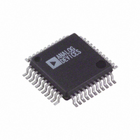
ADV7177KS-REEL Analog Devices Inc, ADV7177KS-REEL Datasheet - Page 27

ADV7177KS-REEL
Manufacturer Part Number
ADV7177KS-REEL
Description
IC DAC VIDEO NTSC 3-CH 44MQFP
Manufacturer
Analog Devices Inc
Type
Video Encoderr
Datasheet
1.ADV7177KSZ-REEL.pdf
(44 pages)
Specifications of ADV7177KS-REEL
Rohs Status
RoHS non-compliant
Applications
Set-Top Boxes, TV
Voltage - Supply, Analog
3 V ~ 3.6 V
Mounting Type
Surface Mount
Package / Case
44-MQFP, 44-PQFP
Adc/dac Resolution
9b
Screening Level
Commercial
Package Type
MQFP
Pin Count
44
Voltage - Supply, Digital
-
Lead Free Status / RoHS Status
Not Compliant
REGISTERS
REGISTER ACCESS
The MPU can write to or read from all of the ADV7177 and
ADV7178 registers except the subaddress register, which is a
write-only register. The subaddress register determines which
register the next read or write operation accesses. All commun-
ications with the part through the bus start with an access to
the subaddress register. A read/write operation is performed
from/to the target address, which then increments to the next
address until a stop command on the bus is performed.
REGISTER PROGRAMMING
This section describes each register, including the subaddress
register, mode registers, subcarrier frequency registers, sub-
carrier phase register, timing registers, closed captioning
extended data registers, closed captioning data registers, and
the NTSC pedestal control registers in terms of configuration.
Subaddress Register (SR7–SR0)
The communications register is an 8-bit, write-only register.
After the parts have been accessed over the bus and a read/write
operation is selected, the subaddress is set up. The subaddress
register determines to/from which register the operation takes
place.
Figure 31 shows the various operations under the control of the
subaddress register. Zero should always be written to SR7–SR6.
Register Select (SR5–SR0)
These bits are set up to point to the required starting address.
SR5
0
0
0
0
0
0
0
0
0
0
0
0
0
0
0
0
0
0
0
0
1
•
•
ZERO SHOULD BE WRITTEN
SR7
SR4
0
0
0
0
0
0
0
0
0
0
0
0
0
0
0
0
1
1
1
1
0
•
•
TO THESE BITS
SR3
SR7–SR6 (00)
0
0
0
0
0
0
0
0
1
1
1
1
1
1
1
1
0
0
0
0
0
•
•
SR2
SR6
0
0
0
0
1
1
1
1
0
0
0
1
1
1
1
0
0
0
0
0
•
•
SR1
0
0
1
1
0
0
1
1
0
0
1
1
0
0
1
1
0
0
1
1
1
•
•
ADV7178 SUBADDRESS REGISTER
SR0
1
0
1
0
1
0
1
0
1
0
1
0
1
0
1
0
1
0
1
0
1
•
•
SR5
MODE REGISTER 0
MODE REGISTER 1
SUBCARRIER FREQ REGISTER 0
SUBCARRIER FREQ REGISTER 1
SUBCARRIER FREQ REGISTER 2
SUBCARRIER FREQ REGISTER 3
SUBCARRIER PHASE REGISTER
TIMING REGISTER 0
CLOSED CAPTIONING EXTENDED DATA– BYTE 0
CLOSED CAPTIONING EXTENDED DATA– BYTE 1
CLOSED CAPTIONING DATA– BYTE 0
CLOSED CAPTIONING DATA– BYTE 1
TIMING REGISTER 1
MODE REGISTER 2
NTSC PEDESTAL CONTROL REG 0 (FIELD 1/3)
NTSC PEDESTAL CONTROL REG 1 (FIELD 1/3)
NTSC PEDESTAL CONTROL REG 2 (FIELD 2/4)
NTSC PEDESTAL CONTROL REG 3 (FIELD 2/4)
MODE REGISTER 3
MACROVISION REGISTER
MACROVISION REGISTER
"
"
SR4
"
"
SR3
SR2
Figure 31. Subaddress Register
Rev. C | Page 27 of 44
SR1
SR5
0
0
0
0
0
0
0
0
0
0
0
0
0
0
0
0
0
0
0
0
0
•
•
SR4
0
0
0
0
0
0
0
0
0
0
0
0
0
0
0
0
1
1
1
1
1
•
•
MODE REGISTER 0 MR0 (MR07–MR00)
Address [SR4–SR0] = 00H
Figure 32 shows the various operations under the control of
Mode Register 0. This register can be read from as well as
written to.
MR0 BIT DESCRIPTION
Output Video Standard Selection (MR01–MR00)
These bits are used to set up the encode mode. The ADV7177/
ADV7178 can be set up to output NTSC, PAL (B, D, G, H, I),
and PAL (M) standard video.
Pedestal Control (MR02)
This bit specifies whether a pedestal is to be generated on
the NTSC composite video signal. This bit is invalid if the
ADV7177/ADV7178 is configured in PAL mode.
Luminance Filter Control (MR04–MR03)
The luminance filters are divided into two sets (NTSC/PAL) of
four filters, low-pass A, low-pass B, notch, and extended. When
PAL is selected, Bits MR03 and MR04 select one of four PAL
luminance filters; likewise, when NTSC is selected, Bits MR03
and MR04 select one of four NTSC luminance filters. The
Typical Performance Characteristics section shows the filters.
RGB Sync (MR05)
This bit is used to set up the RGB outputs with the sync
information encoded on all RGB outputs.
SR0
SR3
0
0
0
0
0
0
0
0
1
1
1
1
1
1
1
1
0
0
0
0
1
•
•
SR2
0
0
0
0
1
1
1
1
0
0
0
0
1
1
1
1
0
0
0
0
1
•
•
SR1
ADV7177 SUBADDRESS REGISTER
0
0
1
1
0
0
1
1
0
0
1
1
0
0
1
1
0
0
1
1
1
•
•
SR0
0
1
0
1
0
1
0
1
0
1
0
1
0
1
0
1
0
1
0
1
0
•
•
MODE REGISTER 0
MODE REGISTER 1
SUBCARRIER FREQ REGISTER 0
SUBCARRIER FREQ REGISTER 1
SUBCARRIER FREQ REGISTER 2
SUBCARRIER FREQ REGISTER 3
SUBCARRIER PHASE REGISTER
TIMING REGISTER 0
CLOSED CAPTIONING EXTENDED DATA– BYTE 0
CLOSED CAPTIONING EXTENDED DATA– BYTE 1
CLOSED CAPTIONING DATA– BYTE 0
CLOSED CAPTIONING DATA– BYTE 1
TIMING REGISTER 1
MODE REGISTER 2
NTSC PEDESTAL CONTROL REG 0 (FIELD 1/3)
NTSC PEDESTAL CONTROL REG 1 (FIELD 1/3)
NTSC PEDESTAL CONTROL REG 2 (FIELD 2/4)
NTSC PEDESTAL CONTROL REG 3 (FIELD 2/4)
MODE REGISTER 3
OSD REGISTER
OSD REGISTER
"
"
"
"
ADV7177/ADV7178


