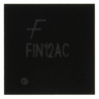
FIN12ACMLX Fairchild Semiconductor, FIN12ACMLX Datasheet - Page 12

FIN12ACMLX
Manufacturer Part Number
FIN12ACMLX
Description
IC SERIALIZER/DESERIALIZER 32MLP
Manufacturer
Fairchild Semiconductor
Series
SerDes™r
Datasheet
1.FIN12ACGFX.pdf
(21 pages)
Specifications of FIN12ACMLX
Function
Serializer/Deserializer
Data Rate
560Mbps
Input Type
LVCMOS
Output Type
LVCMOS
Number Of Inputs
12
Number Of Outputs
12
Voltage - Supply
1.65 V ~ 3.6 V
Operating Temperature
-30°C ~ 70°C
Mounting Type
Surface Mount
Package / Case
32-MLP
Lead Free Status / RoHS Status
Lead free / RoHS Compliant
Other names
FIN12ACMLX
FIN12ACMLXTR
FIN12ACMLXTR
Available stocks
Company
Part Number
Manufacturer
Quantity
Price
Part Number:
FIN12ACMLX
Manufacturer:
FAIRCHILD/仙童
Quantity:
20 000
Part Number:
FIN12ACMLX.
Manufacturer:
FAI
Quantity:
20 000
FIN12AC Rev. 1.1.2
© 2006 Fairchild Semiconductor Corporation
Power Supply Currents
The worst-case test pattern produces a maximum toggling of internal digital circuits, CTL I/O and LVCMOS I/O with the
PLL operating at the reference frequency unless otherwise specified. Maximum power is measured at the maximum
V
DD
I
I
Symbol
DD_SER1
DD_DES1
I
DD_PD
I
I
I
I
DDA1
DDA2
DDS1
DDS2
values. Minimum values are measured at the minimum V
V
V
Current
V
V
Current
V
I
14:1 Dynamic Serializer
Power Supply Current
I
14:1 Dynamic Deserializer
Power Supply Current
I
DD_PD
DD_SER1
DD_DES1
DDA
DDA
DDS
DDS
DD
Power-Down Supply Current
Serializer Static Supply Current
Deserializer Static Supply
Serializer Static Supply Current
Deserializer Static Supply
= I
= I
= I
DDA
DDA
DDA
Parameter
+ I
+ I
+ I
DDS
DDS
DDS
+ I
DDP
+ I
+ I
DDP
DDP
All DP and Control Inputs at 0V or
V
DIR = 1
All DP and Control Inputs at 0V or
V
DIR = 0
All DP and Control Inputs at 0V or
V
DIR = 1
All DP and Control Inputs at 0V or
V
DIR = 0
S1 = S2 = 0
All Inputs at GND or V
CKREF = STROBE
DIRI = H
Figure 10
CKREF = STROBE
DIRI = L
Figure 10
DD
DD
DD
DD
NOCKREF, S2 = 0, S1 = 1,
NOCKREF, S2 = 0, S1 = 1,
NOCKREF, S2 = 0, S1 = 1,
NOCKREF, S2 = 0, S1 = 1,
12
Test Conditions
DD
values. Typical values are measured at V
S2 = H
S1 = L
S2 = H
S1 = H
S2 = L
S1 = H
S2 = H
S1 = L
S2 = H
S1 = H
S2 = L
S1 = H
DD
5
14MHz
10MHz
28MHz
20MHz
40MHz
5
14MHz
10MHz
28MHz
20MHz
40MHz
MHz
MHz
Min.
Typ.
15.0
17.0
11.0
17.0
10.0
11.5
437
528
4.4
5.5
1.0
8.5
9.5
6.5
7.5
7.0
8.5
www.fairchildsemi.com
Max. Unit
DD
= 2.5V.
mA
mA
mA
mA
µA
µA
µA


