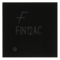
FIN12ACMLX Fairchild Semiconductor, FIN12ACMLX Datasheet - Page 13

FIN12ACMLX
Manufacturer Part Number
FIN12ACMLX
Description
IC SERIALIZER/DESERIALIZER 32MLP
Manufacturer
Fairchild Semiconductor
Series
SerDes™r
Datasheet
1.FIN12ACGFX.pdf
(21 pages)
Specifications of FIN12ACMLX
Function
Serializer/Deserializer
Data Rate
560Mbps
Input Type
LVCMOS
Output Type
LVCMOS
Number Of Inputs
12
Number Of Outputs
12
Voltage - Supply
1.65 V ~ 3.6 V
Operating Temperature
-30°C ~ 70°C
Mounting Type
Surface Mount
Package / Case
32-MLP
Lead Free Status / RoHS Status
Lead free / RoHS Compliant
Other names
FIN12ACMLX
FIN12ACMLXTR
FIN12ACMLXTR
Available stocks
Company
Part Number
Manufacturer
Quantity
Price
Part Number:
FIN12ACMLX
Manufacturer:
FAIRCHILD/仙童
Quantity:
20 000
Part Number:
FIN12ACMLX.
Manufacturer:
FAI
Quantity:
20 000
FIN12AC Rev. 1.1.2
© 2006 Fairchild Semiconductor Corporation
AC Electrical Characteristics
Characteristics at recommended over-supply voltage and operating temperature ranges, unless otherwise specified.
Typical values are given for V
device and negative values refer to current flowing out of pins. Voltages are referenced to GROUND unless otherwise
specified (except ΔV
Serializer Input Operating Conditions
Serializer AC Electrical Characteristics
PLL AC Electrical Characteristics
Deserializer AC Electrical Characteristics
Symbol
t
t
t
t
t
TPLLD0
TPLLD1
t
t
t
t
TPLLS0
t
t
t
t
t
ƒ
CPWH
CPWL
SPWH
f
RCOP
RCOH
t
t
t
TCCD
SPOS
RCOL
t
ROLH
ROHL
CLKT
MAX
HTC
PDV
TCP
STC
REF
CKREF Clock Period
(5MHz – 40MHz)
CKREF Frequency Relative to
STROBE Frequency
CKREF Clock High Time
CKREF Clock Low Time
LVCMOS Input Transition Time
STROBE Pulse Width HIGH/LOW
Maximum Serial Data Rate
Transmitter Clock Input to Clock
Output Delay
CKSO Position Relative to DS
Serializer Phase-Lock Loop
Stabilization Time
PLL Disable Time Loss of Clock
PLL Power-Down Time
Deserializer Clock Output
(CKP OUT) Period
CKP OUT Low Time
CKP OUT High Time
Data Valid to CKP LOW
Output Rise Time (20% to 80%)
Output Fall Time (80% to 20%)
DP
DP
(n)
(n)
Setup to STROBE
Hold to STROBE
OD
Parameter
and V
OD
DD
(6)
).
(4)
(6)
= 2.775V and T
(3)
CKREF = STROBE
Figure 13
CKREF does not =
STROBE
Figure 13
Figure 13
CKREF x 14
DIRI = 1
Figure 3 (f = 5MHz)
DIRI = 1, a=(1/f)/14
CKREF = STROBE,
Figure 17
Figure 15
Figure 18
Figure 19
Figure 14
Figure 14 (Rising Edge Strobe)
Serializer source STROBE =
CKREF
where a = (1/f)/14
Figure 14 (Rising Edge Strobe)
where a = (1/f)/14
C
Figure 11
A
L
= 5pF
= 25°C. Positive current values refer to the current flowing into
Test Conditions
13
S2=1 S1=0
S2=1 S1=1
S2=0 S1=1
S2=1 S1=0
S2=1 S1=0
S2=0 S1=1
S2=0 S1=1
S2=1 S1=0
S2=1 S1=1
(T x 4)/14
23a+1.5
f
STROBE
Min.
1.1 x
7a–3
7a–3
7a–3
71.0
35.0
25.0
-200
17.8
280
140
0.2
0.2
2.5
2.0
70
Typ.
0.5
0.5
3.5
3.5
(T x 12)/14
21a+6.5
Max.
7a+3
7a+3
7a+3
50.0
90.0
30.0
20.0
200
100
540
196
392
200
200
200
7.0
7.0
www.fairchildsemi.com
40
14
28
Unit
Mb/s
MHz
ns
ns
ns
ns
ns
ns
ps
µs
µs
ns
ns
ns
ns
ns
ns
ns
T
T


