FIN24CMLX Fairchild Semiconductor, FIN24CMLX Datasheet - Page 11
FIN24CMLX
Manufacturer Part Number
FIN24CMLX
Description
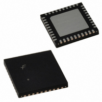
IC SERIALIZER/DESERIALZR 40MLP
Manufacturer
Fairchild Semiconductor
Series
SerDes™r
Datasheet
1.FIN24CGFX.pdf
(25 pages)
Specifications of FIN24CMLX
Function
Serializer/Deserializer
Data Rate
520Mbps
Input Type
LVCMOS
Output Type
LVCMOS
Number Of Inputs
20
Number Of Outputs
20
Voltage - Supply
1.65 V ~ 3.6 V
Operating Temperature
-30°C ~ 70°C
Mounting Type
Surface Mount
Package / Case
40-MLP
Lead Free Status / RoHS Status
Lead free / RoHS Compliant
Available stocks
Company
Part Number
Manufacturer
Quantity
Price


©2005 Fairchild Semiconductor Corporation
FIN24C Rev. 1.0.2
PLL Circuitry
The CKREF input signal is used to provide a reference to
the PLL. The PLL generates internal timing signals capa-
ble of transferring data at 26 times the incoming CKREF
signal. The output of the PLL is a bit clock sent with the
serial data stream.
There are two ways to disable the PLL: by entering the
Application Mode Diagrams
Figure 11 shows basic operation when a pair of SerDes is configured in an unidirectional operation mode.
In Master Operation, the device:
1. Is configured as a serializer at power-up based on the
2. Accepts CKREF_M word clock and generate a bit
3. Receives parallel data on the rising edge of
4. Generates and transmits serialized data on the
5. Generates an embedded word clock for each strobe
Figure 10. Bi-Directional Differential I/O Circuitry
value of the DIRI signal.
clock with embedded word boundary. This bit clock is
sent to the slave device through the CKSO port.
STROBE_M.
signal.
Deserializer
Serializer
DS signals source synchronous with CKSO.
STROBE_M
From
DP[1:22]_M
CKREF_M
Master Device Operating as a Serializer
To
Control
From
Figure 11. Simplified Block Diagram for Unidirectional Serializer and Deserializer
+
–
S2 = S1 = “0”
DIR = “1”
+
–
PLL
Serializer
Control
Serializer
BIT CK
Gated
Termination
(DS Pins Only)
Gen.
MODE = 3: Unidirectional Data Transfer
DS+
DS-
CKSO
+
–
+
–
DS
11
CKSI
+
–
+
–
Mode 0 state (S1 = S2 = 0) or upon detecting a LOW on
both the S1 and S2 signals. Any of the other modes are
entered by asserting either S1 or S2 HIGH and by pro-
viding a CKREF signal. The PLL powers up and goes
through a lock sequence. Wait the specified number of
clock cycles prior to capturing valid data into the parallel
port. When the µSerDes chipset transitions from a
power-down state (S1, S2 = 0, 0) to a powered state
(example S1, S2 = 1, 1), CKP on the deserializer transi-
tions LOW for a short duration, then returns HIGH. Fol-
lowing this, the signal level of the deserializer at CKP
corresponds to the serializer signal levels.
An alternate way of powering down the PLL is by stop-
ping the CKREF signal either HIGH or LOW. Internal cir-
cuitry detects the lack of transitions and shuts the PLL
and serial I/O down. Internal references, however, are
not disabled, allowing the PLL to power-up and re-lock in
a lesser number of clock cycles than when exiting Mode
0. When a transition is seen on the CKREF signal, the
PLL is reactivated.
In Slave Operation, the device:
1. Is configured as a deserializer at power-up based on
2. Accepts an embedded word boundary bit clock on
3. Deserializes the DS data stream using the CKSI input
4. Writes parallel data onto the DP_S port and generates
Slave Device Operating as a Deserializer
the value of the DIRI signal.
CKSI.
clock.
the CKP_S. CKP_S is only generated when a valid
data word occurs.
Deserializer
Deserializer
Control
Work CK
Gen
S2 = S1 = “0”
DIR = “0”
CKP_S
DP[1:20, 23:24]_S
www.fairchildsemi.com
Related parts for FIN24CMLX
Image
Part Number
Description
Manufacturer
Datasheet
Request
R

Part Number:
Description:
Serdes Low Voltage 24-bit Bi-directional Serializer/deserializer
Manufacturer:
Fairchild Semiconductor
Datasheet:
Part Number:
Description:
Fairchild Semiconductor [IGBT MODULE]
Manufacturer:
Fairchild Semiconductor
Datasheet:

Part Number:
Description:
Discrete Semiconductor Modules
Manufacturer:
Fairchild Semiconductor
Part Number:
Description:
Discrete Semiconductor Modules
Manufacturer:
Fairchild Semiconductor
Part Number:
Description:
This N-Channel MOSFET is produced using Fairchild Semiconductor’s advanced Power Trench® process
Manufacturer:
Fairchild Semiconductor
Datasheet:
Part Number:
Description:
This N-Channel MOSFET is produced using Fairchild Semiconductor’s advanced Power Trench® process
Manufacturer:
Fairchild Semiconductor
Datasheet:
Part Number:
Description:
This N-Channel MOSFET is produced using Fairchild Semiconductor’s advanced PowerTrench® process
Manufacturer:
Fairchild Semiconductor
Datasheet:
Part Number:
Description:
This N-Channel MOSFET is produced using Fairchild Semiconductor’s advanced PowerTrench® process
Manufacturer:
Fairchild Semiconductor
Datasheet:
Part Number:
Description:
This N-Channel MOSFET is produced using Fairchild Semiconductor’s advanced Power Trench® process
Manufacturer:
Fairchild Semiconductor
Datasheet:
Part Number:
Description:
This N-Channel logic Level MOSFETs are produced using Fairchild Semiconductor‘s advanced Power Trench® process that has been special tailored to minimize the on-state resistance and yet maintain superior switching performance
Manufacturer:
Fairchild Semiconductor
Datasheet:
Part Number:
Description:
This N-Channel MOSFET is produced using Fairchild Semiconductor’s advanced Power Trench® process
Manufacturer:
Fairchild Semiconductor
Datasheet:
Part Number:
Description:
This N-Channel SyncFET™ is produced using Fairchild Semiconductor’s advanced PowerTrench® process
Manufacturer:
Fairchild Semiconductor
Datasheet:
Part Number:
Description:
This N-Channel SyncFET™ is produced using Fairchild Semiconductor’s advanced PowerTrench® process
Manufacturer:
Fairchild Semiconductor
Datasheet:
Part Number:
Description:
This N-Channel SyncFET™ is produced using Fairchild Semiconductor’s advanced PowerTrench® process
Manufacturer:
Fairchild Semiconductor
Datasheet:
Part Number:
Description:
This N-Channel logic Level MOSFETs are produced using Fairchild Semiconductor‘s advanced Power Trench® process that has been special tailored to minimize the on-state resistance and yet maintain superior switching performance
Manufacturer:
Fairchild Semiconductor
Datasheet: